Leakage effects in mos-fets
âĒDownload as PPTX, PDFâĒ
2 likesâĒ3,594 views

this ppt discuss abt the various sources of power dissipation in cmos gates..such as leakage current and its various mechanisms..


Leakage effects in mos-fets
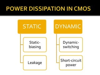
- 3. ïĄ Dynamic switching power dissipation is caused by charging capacitances in the circuit. ïĄ The dynamic switching power dissipation was the dominant factor compared with other components of power dissipation in digital CMOS circuits for technologies up to 0.18Ξm, where it is about 90% of total circuit dissipation.
- 4. ï§ Shortâcircuit power is the second source of total power dissipation ï§ During a transient on the input signal, there will be a period in which both NMOS and PMOS transistor will conduct simultaneously, causing a current flow through the direct path existing between power supply and ground terminals. This short circuit current usually happens for very small intervals. ï§ In a static CMOS inverter this current is proportional to the input ramp, the output load, and the transistors size
- 6. ïĄ Real systems present degraded voltage levels feeding CMOS gates and a current flow from the power supply to ground nodes is observed.This flow is known as static biasing current. Degraded voltage level at the input node of an CMOS inverter results in static biasing power consumption.
- 7. ïĄ Static current that flows fromVdd to ground nodes,without degraded inputs is known as leakage power. ïĄ These are the three major types of leakage mechanisms: subthreshold, gate oxide and reverse-bias pn-junction leakage (BTBT âband-to-band tunneling). ïĄ In addition to these three major leakage components, there are other ones like gate-induced drain leakage(GIDL) and punchthrough current.Those components can be neglected in normal modes of operation.
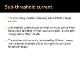
- 9. ïĄ TheVth scaling results in increasing subthreshold leakage currents. ïĄ Subthreshold current occurs between drain and source when transistor is operating in weak inversion region, i.e., the gate voltage is lower than theVth. ïĄ The subthreshold current is dominated by diffusion current and it depends exponentially on both gate-to-source and threshold voltage.
- 10. The subthreshold leakage current for a MOSFET device can be expressed as:
- 11. ïĄ To control the short channel effects, oxide thickness must also become thinner in each technology generation. ïĄ Aggressive scaling of the oxide thickness, in turn, gives rise to high electric field, resulting in a high direct-tunneling current through transistor gate insulator.
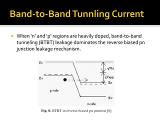
- 13. ïĄ When ânâ and âpâ regions are heavily doped, band-to-band tunneling (BTBT) leakage dominates the reverse biased pn junction leakage mechanism.
- 14. Body- biasing Power gating Dual-threshold CMOS Supply voltage Scaling Transistor Stacking Effect
- 15. ïĄ As power consumption is directly proportional to the square of the power supply voltage, MOS transistor has been scaled to maintain performance at reduced supply voltage. ïĄ Transistor threshold voltage is also reduced to avoid short channel effect, resulting in a substantial increasing in leakage currents when transistor scaling into nanometer dimensions. ïĄ Standby current becomes a significant portion of the total IC power consumption, being a challenge for designers and a critical factor in low-power circuits.
- 16. ïĄ Leakage mechanisms and reduction techniques have been reviewed,in this ppt.. ïĄ Accurate models to estimate subthreshold leakage have to treat the stack effect. Gate leakage estimation, on the other hand, is usually based on transistor biasing.