
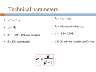

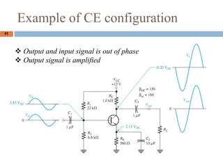
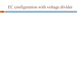
![Collector-feedback bias
BE loop:
ˇ®
(1) Vcc- Ic RC ¨C IBRB ¨C UBE ¨C IERE =0
(2) IC= ¦Â *IB ; IE ? IC
c c
(3) KCL at C: IC= IB + I ˇ® ˇú I ˇ® = IC - IB
= (¦Â-1)IB
(1)+(2)+(3)
ˇú IB= (Vcc - UBE)/[RB+ ¦Â(Rc+Re)]
CE loop:
UCE = Vcc ¨C IC (RC+RE)
Quite stable
30](https://image.slidesharecdn.com/20241chapter1bjt-250315141833-3ad770e8/85/20241_Chapter-1eg-regdfgdfhdfh-dfhdf-hd_BJT-pdf-30-320.jpg)

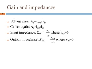


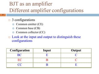
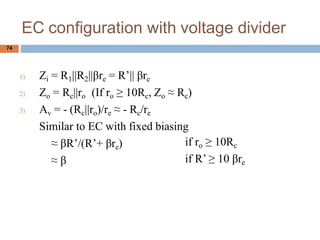
![EC configuration with fixed biasing
1) Zi = Rb||¦Âre
2) Zo = Rc||ro
if Rb ˇÝ 10¦Âre,
if ro ˇÝ 10Rc,
Zi ˇÖ ¦Âre
Zo ˇÖ Rc
3) Av = - (Rc||ro)/re ˇÖ - Rc/re
(¦Â appered in re)
Ui & Uo out of phase180o
4) Ai = ¦ÂRbro / [(ro+Rc)(Rb+¦Âre)] ˇÖ ¦Â
(Ii current source. Io collector current)
70](https://image.slidesharecdn.com/20241chapter1bjt-250315141833-3ad770e8/85/20241_Chapter-1eg-regdfgdfhdfh-dfhdf-hd_BJT-pdf-69-320.jpg)

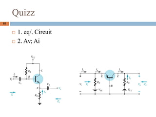
![1) Zi = Rb || [¦Âre+(¦Â+1)Re] ˇÖ Rb || ¦Â(re+Re)
High input impedance
2) Zo = Re||re ˇÖ re where Re >> re
Low output impedance
3) Av = Re/(Re+re) ˇÖ 1
Inphase with input and smaller amplitude
=> ˇ°emitter connectionˇ±
4) Ai = - ¦ÂRb/[Rb+ ¦Â(re+Re)]
Application: Buffer
91
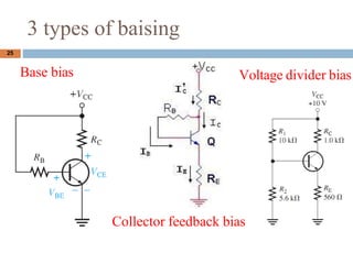
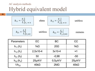
CC configuration with fixed biasing](https://image.slidesharecdn.com/20241chapter1bjt-250315141833-3ad770e8/85/20241_Chapter-1eg-regdfgdfhdfh-dfhdf-hd_BJT-pdf-90-320.jpg)


20241_Chapter 1eg regdfgdfhdfh dfhdf hd_BJT.pdf
- 1. Chapter 1: Bipolar Junction Transistor (BJT) Assoc. Prof. Pham Nguyen Thanh Loan September, 2024
- 2. Contents ? Structure and operation of BJT ? Different configurations of BJT ? Characteristic curves ? DC biasing method and analysis ? Base bias ? Collector-feedback bias ? Voltage divider bias ? AC signal analysis ? Impact of other parameters (temperature, leakage currents) 2 The content of these slides are based on the book titled ˇ°Electronics Devices and Circuit theory of Robert Boylestadˇ±
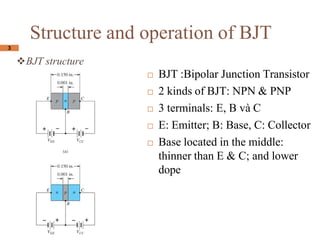
- 3. Structure and operation of BJT ?BJT structure ? BJT :Bipolar Junction Transistor ? 2 kinds of BJT: NPN & PNP ? 3 terminals: E, B v¨¤ C ? E: Emitter; B: Base, C: Collector ? Base located in the middle: thinner than E & C; and lower dope 3
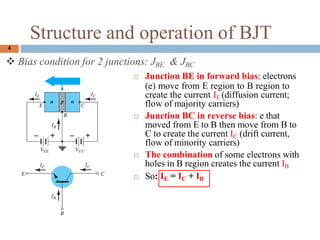
- 4. ? So: IE = IC + IB ? Bias condition for 2 junctions: JBE & JBC ? Junction BE in forward bias: electrons (e) move from E region to B region to create the current IE (diffusion current; flow of majority carriers) ? Junction BC in reverse bias: e that moved from E to B then move from B to C to create the current IC (drift current, flow of minority carriers) ? The combination of some electrons with holes in B region creates the current IB 4 Structure and operation of BJT
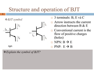
- 5. ? 3 terminals: B, E v¨¤ C ? Arrow instructs the current direction between B & E ? Conventional current is the flow of positive charges (holes) ? NPN: B ˇú E ? PNP: E ˇú B ?BJT symbol IB IC IE 5 Structure and operation of BJT ?Explain the symbol of BJT?
- 6. 6 Technical parameters ? IC = ¦ÁIE + ICBO ? IC ˇÖ ¦ÁIE (neglect leakage ICBO) ? ¦Á = 0.9 ˇÂ0.998. ? ¦Á is DC current transfer coefficient ? IE = IC + IB ? IC = ¦ÂIB ? ¦Â = 100 ˇÂ 200 (may be higher) ? ¦Â is DC current gain ¦Á = ¦Â ¦Â + 1
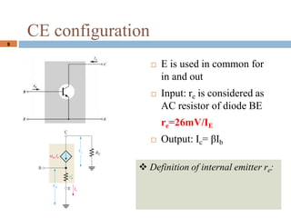
- 7. 7 BJT as an amplifier Different amplifier configurations ? 3 configurations ? Common emitter (CE) ? Common base (CB) ? Common collector (CC) ? Look at the input and output to distinguish these configurations Configuration Input Output BC E C EC B C CC B E
- 8. BJT as an amplifier ? CE with voltage divider biasing 8 ? CC with voltage divider biasing ? CB with fixed biasing B E C E B C
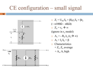
- 9. 9 CE configuration ? E is used in common for in and out ? Input: re is considered as AC resistor of diode BE re=26mV/IE ? Output: Ic= ¦ÂIb ? Definition of internal emitter re:
- 10. 10 CE configuration ¨C small signal ? Zi = Ube/Ib ˇÖ ¦ÂIbre/Ib ˇÖ ¦Âre (~ n100¦¸ ¨C nK¦¸) ? Zo = ro ˇú ˇŢ (ignore in re model) ? Av = - RL/re (roˇú ˇŢ) ? Ai = Ic/Ib = ¦Â ? Characteristics + Zi, Zo average + Av, Ai high
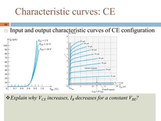
- 11. 11 Characteristic curves: CE ? Input and output characteristic curves of CE configuration 11 ?Explain why VCE increases, IB decreases for a constant VBE?
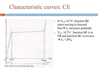
- 12. 12 Characteristic curves: CE ? 0<VCE<0.7V: Junction BE starts moving to forward biasˇú IC increases gradually ? VCE >0.7V: Junction BE is in FB and Junction BC in reverse ˇú IC = ¦Â*IB
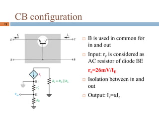
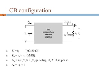
- 13. 13 CB configuration ? B is used in common for in and out ? Input: re is considered as AC resistor of diode BE re=26mV/IE ? Isolation between in and out ? Output: Ic=¦ÁIe
- 14. 14 1) Zi = re (n¦¸-50 ¦¸) 2) Zo = ro ˇÖ ˇŢ (nM¦¸) 3) Av = ¦ÁRL/re ˇÖ RL/re quite big, Uo & Ui in phase 4) Ai = -¦Á ˇÖ 1 CB configuration
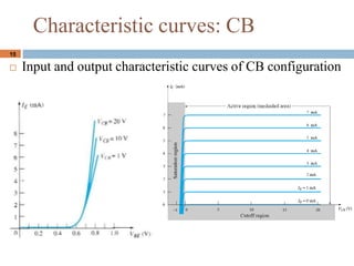
- 15. 15 Characteristic curves: CB ? Input and output characteristic curves of CB configuration
- 16. 16 CC configuration ? Similar to CE configuration ? Refer to Electronic Devices ¨C Thomas Floyd
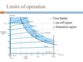
- 17. Limits of operation ? Two limits: ? cut-off region ? Saturation region 17
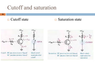
- 18. Cutoff and saturation ? Cutoff state ? Saturation state 18
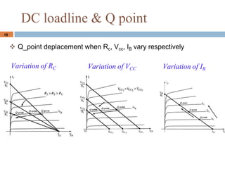
- 19. 19 ? Q_point deplacement when Rc, Vcc, IB vary respectively DC loadline & Q point Variation of RC Variation of VCC Variation of IB
- 20. DC power vs. AC signal 20 DCpower AC signal
- 21. Example of CE configuration 21 ? Output and input signal is out of phase ? Output signal is amplified
- 22. DC bias: DC operating point & DC load line 22
- 23. DC bias ? A transistor must be properly biased in order to operate as an amplifier ? DC bias can be considered as supply power to BJT so that ? NPN: VE < VB < VC (JE: in Forward; JC: in Reverse bias) ? PNP: VE > VB > VC ? DC bias is characterized by Q-point (DC operating point) and DC load line 23
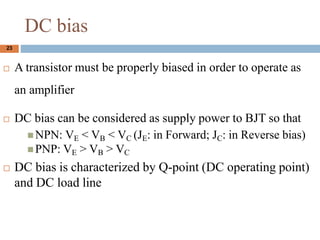
- 24. DC bias ? NOTES: REMEMBER some equations: VBE ˇÖ 0,6 ˇÂ 0,7V (Si) ; 0,2 ˇÂ 0,3(Ge) IC ˇÖ ¦ÁIE IE = IC + IBIC = ¦ÂIB ? There 3 types of bias circuits ? Base bias ? Collector-feedback bias ? Voltage divider bias ? Question: How many amplifier circuits can be designed? 24
- 25. 3 types of baising Base bias 25 Collector feedback bias Voltage divider bias
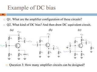
- 26. Example of DC bias 26 ? Q1. What are the amplifier configuration of these circuits? ? Q2. What kind of DC bias? And then draw DC equivalent circuit. (a) (b) (c) ? Question 3: How many amplifier circuits can be designed?
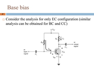
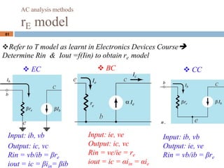
- 27. ? Consider the analysis for only EC configuration (similar analysis can be obtained for BC and CC) 27 Base bias
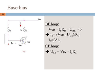
- 28. Base bias BE loop: Vcc ¨C IBRB ¨C UBE = 0 ? IB= (Vcc - UBE)/RB IC=¦Â*IB CE loop: ? UCE = Vcc - ICRC 28
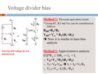
- 29. Voltage divider bias Current and voltage do not depend on ¦Â 29 Method 1: Thevenin equivalent circuit: * Group R1, R2 and Vcc can be considered as follows: RBB=R1//R2 VBB= Vcc * R2/(R1+R2) ? Now it is similar to base-bias analysis Method 2: Approximative analysis If ¦Â*R ˇÝ 10R -> I ˇÖ I 2 2 2 1 ? VB=Vcc*R2/(R1+R2) ? VE=VB-VBE ? Ic ˇÖ IE=VE/RE ? VCE=Vcc- IC(RC+RE)
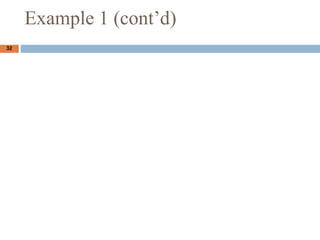
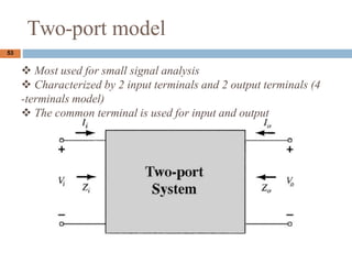
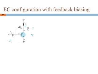
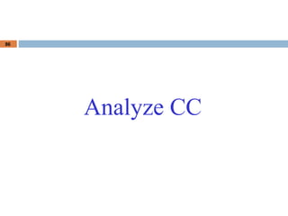
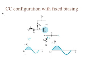
- 30. Collector-feedback bias BE loop: ˇ® (1) Vcc- Ic RC ¨C IBRB ¨C UBE ¨C IERE =0 (2) IC= ¦Â *IB ; IE ? IC c c (3) KCL at C: IC= IB + I ˇ® ˇú I ˇ® = IC - IB = (¦Â-1)IB (1)+(2)+(3) ˇú IB= (Vcc - UBE)/[RB+ ¦Â(Rc+Re)] CE loop: UCE = Vcc ¨C IC (RC+RE) Quite stable 30
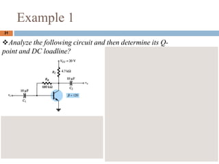
- 31. Example 1 31 ?Analyze the following circuit and then determine its Q- point and DC loadline?
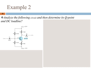
- 33. Example 2 33 ?Analyze the following circuit and then determine its Q-point and DC loadline?
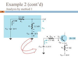
- 34. 34 Example 2 (contˇŻd) Analysis by method 1
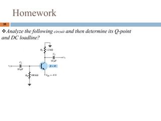
- 35. Homework 35 ?Analyze the following circuit and then determine its Q-point and DC loadline?
- 36. Homework 36 ?Analyze the following circuit and then determine its Q-point and DC loadline?
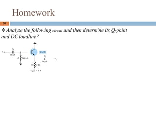
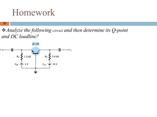
- 37. Homework 37 ?Analyze the following circuit and then determine its Q-point and DC loadline?
- 38. Working on your 1st in-class assignment 38
- 39. AC analysis (Small signal analysis) 39
- 40. Small signal analysis ? Small signal analysis: ? Small signal refers to AC signal with small amplitude that take up a relatively small percentage of an amplifierˇŻs operation range (compared to DC power supply) ? The operation region on amplifier should be in linear ? BJT model for small signal analysis ? Represent the BJT by an equivalent circuit that allows to visualize and analyze the operation of BJT as an amplifier 40
- 41. Example of CE configuration 41 ? Output and input signal is out of phase ? Output signal is amplified
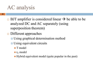
- 43. AC equivalent circuit ? 1. Setting all DC sources to zero ? 2. Replacing all capacitors by a short-circuit equivalent (wire) ? 3. Regrouping all elements (resistors) in parallel (introduced by step 1 and 2) ? 4. Redrawing the network in a more convenient and logical form 43
- 44. AC analysis ? BJT amplifier is considered linear ˇú be able to be analyzed DC and AC separately (using superposition theorem) ? Different approaches ? Using graphical determination method ? Using equivalent circuits ? T model ? rE model ? Hybrid equivalent model (quite popular in the past) 44
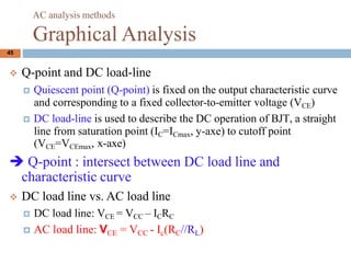
- 45. ? Q-point and DC load-line ? Quiescent point (Q-point) is fixed on the output characteristic curve and corresponding to a fixed collector-to-emitter voltage (VCE) ? DC load-line is used to describe the DC operation of BJT, a straight line from saturation point (IC=ICmax, y-axe) to cutoff point (VCE=VCEmax, x-axe) ? Q-point : intersect between DC load line and characteristic curve ? DC load line vs. AC load line ? DC load line: VCE = VCC ¨C ICRC ? AC load line: VCE = VCC - Ic(RC//RL) 45 AC analysis methods Graphical Analysis
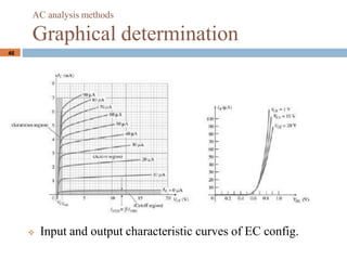
- 46. 46 AC analysis methods Graphical determination ? Input and output characteristic curves of EC config.
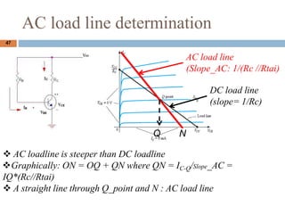
- 47. AC load line determination 47 AC load line (Slope_AC: 1/(Rc //Rtai) DC load line (slope= 1/Rc) Q N ? AC loadline is steeper than DC loadline ?Graphically: ON = OQ + QN where QN = IC-Q/Slope_AC = IQ*(Rc//Rtai) ? A straight line through Q_point and N : AC load line
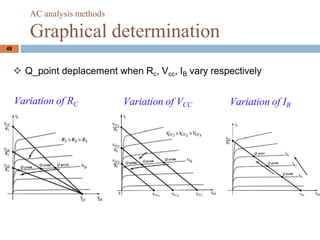
- 48. 48 ? Q_point deplacement when Rc, Vcc, IB vary respectively AC analysis methods Graphical determination Variation of RC Variation of VCC Variation of IB
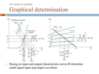
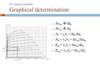
- 49. 49 ? Basing on input and output characteristic curvesˇú determine small signal input and output waveform AC analysis methods Graphical determination
- 50. 50 ? ¦¤vbe ˇú ¦¤ib ? ¦¤vce ˇú ¦¤ic ? Ai = io/ii = ¦¤ic/¦¤ib ? AV= vo/vi = ¦¤vce/¦¤vbe ? Zin = vi/ii = ¦¤vbe/¦¤ib ? Zout = vo/io = ¦¤vce/¦¤ic AC analysis methods Graphical determination
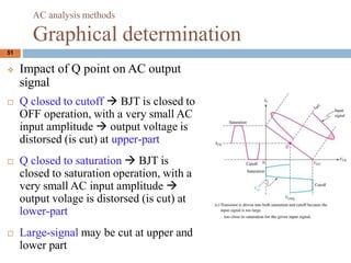
- 51. ? Impact of Q point on AC output signal ? Q closed to cutoff ˇú BJT is closed to OFF operation, with a very small AC input amplitude ˇú output voltage is distorsed (is cut) at upper-part ? Q closed to saturation ˇú BJT is closed to saturation operation, with a very small AC input amplitude ˇú output volage is distorsed (is cut) at lower-part ? Large-signal may be cut at upper and lower part 51 AC analysis methods Graphical determination
- 52. AC analysis ? BJT amplifier is considered linear ˇú be able to be analyzed DC and AC separately (using superposition theorem) ? Different approaches ? Using graphical determination method ? Using equivalent circuits ? T model ? rE model ? Hybrid equivalent model (quite popular in the past) 52
- 53. Two-port model 53 ? Most used for small signal analysis ? Characterized by 2 input terminals and 2 output terminals (4 -terminals model) ? The common terminal is used for input and output
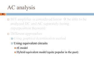
- 54. Remind: AC equivalent circuit ? 1. Setting all DC sources to zero ? 2. Replacing all capacitors by a short-circuit equivalent (wire) ? 3. Regrouping all elements (resistors) in parallel (introduced by step 1 and 2) ? 4. Redrawing the network in a more convenient and logical form 54 ` ` `
- 55. 55 ? Equivalent circuit after step 1 and 2 Remind: AC equivalent circuit ????????? ????????? ? Equivalent circuit after step 3 and 4
- 56. AC analysis ? BJT amplifier is considered linear ˇú be able to be analyzed DC and AC separately (using superposition theorem) ? Different approaches ? Using graphical determination method ? Using equivalent circuits ? rE model ? Hybrid equivalent model (quite popular in the past) 56
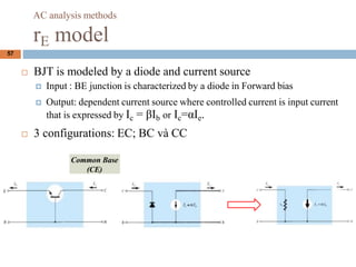
- 57. ? BJT is modeled by a diode and current source ? Input : BE junction is characterized by a diode in Forward bias ? Output: dependent current source where controlled current is input current that is expressed by Ic = ¦ÂIb or Ic=¦ÁIe. ? 3 configurations: EC; BC v¨¤ CC 57 AC analysis methods rE model Common Base (CE)
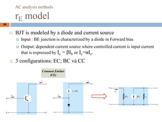
- 58. ? BJT is modeled by a diode and current source ? Input : BE junction is characterized by a diode in Forward bias ? Output: dependent current source where controlled current is input current that is expressed by Ic = ¦ÂIb or Ic=¦ÁIe. ? 3 configurations: EC; BC v¨¤ CC 58 AC analysis methods rE model Common Emitter (CE)
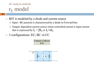
- 59. ? BJT is modeled by a diode and current source ? Input : BE junction is characterized by a diode in Forward bias ? Output: dependent current source where controlled current is input current that is expressed by Ic = ¦ÂIb or Ic=¦ÁIe. ? 3 configurations: EC; BC v¨¤ CC 59 AC analysis methods rE model Common Collector (CC)
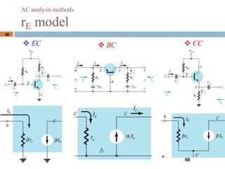
- 60. 60 ? EC ? BC ? CC c e b e c e c 60 AC analysis methods rE model
- 61. 61 ? EC ? BC ? CC c e b e c c e Input: ib, vb Output: ic, vc Rin = vb/ib = ¦Âre iout = ic = ¦Âiin= ¦Âib ?Refer to T model as learnt in Electronics Devices Course? Determine Rin & Iout =f(Iin) to obtain re model Input: ie, ve Output: ic, vc Rin = ve/ie = re iout = ic = ¦Áiin = ¦Áie Input: ib, vb Output: ie, ve Rin = vb/ib = ¦Âre AC analysis methods rE model
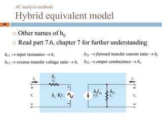
- 62. ? U & I relation: Ui=h11Ii+h12Uo Io=h21Ii+h22Uo ? hij is determined at a given operating point (can be different from Q_point) ? Index e (or b, c) illustrated for CE topology (or CB, CC) ? Hybrid parameters for 2N4400 62 AC analysis methods Hybrid equivalent model 2 ports Iv Ir Uv Ur
- 63. 63 AC analysis methods Hybrid equivalent model Parameters EC BC CC h11 (hi) 1k¦¸ 20¦¸ 1k¦¸ h12 (hr) 2,5x10⁻⁴ 3x10⁻⁴ ˇÖ1 h21 (hf) 50 -0,98 -50 h22 (ho) 25¦ĚA/V 0,5¦ĚA/V 25¦ĚA/V 1/h22 40k¦¸ 2M¦¸ 40k¦¸
- 64. ? Other names of hij ? Read part 7.6, chapter 7 for further understanding 64 AC analysis methods Hybrid equivalent model hi h V r i hfIin h0
- 65. 66 Analyze EC AC analysis methods rE model
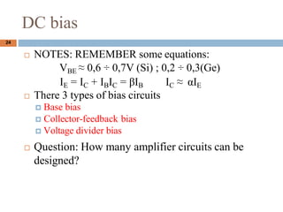
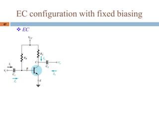
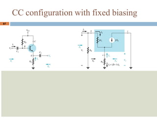
- 66. 67 ? EC EC configuration with fixed biasing
- 67. 68 EC configuration with fixed biasing 68
- 68. 69 EC configuration with fixed biasing 69
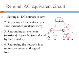
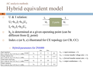
- 69. EC configuration with fixed biasing 1) Zi = Rb||¦Âre 2) Zo = Rc||ro if Rb ˇÝ 10¦Âre, if ro ˇÝ 10Rc, Zi ˇÖ ¦Âre Zo ˇÖ Rc 3) Av = - (Rc||ro)/re ˇÖ - Rc/re (¦Â appered in re) Ui & Uo out of phase180o 4) Ai = ¦ÂRbro / [(ro+Rc)(Rb+¦Âre)] ˇÖ ¦Â (Ii current source. Io collector current) 70
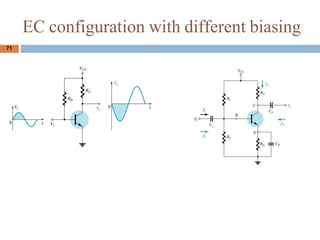
- 70. EC configuration with different biasing 71
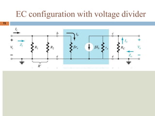
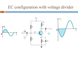
- 71. EC configuration with voltage divider 72
- 72. 73 EC configuration with voltage divider
- 73. 1) Zi = R1||R2||¦Âre = RˇŻ|| ¦Âre 2) Zo = Rc||ro (If ro ˇÝ 10Rc, Zo ˇÖ Rc) 3) Av = - (Rc||ro)/re ˇÖ - Rc/re Similar to EC with fixed biasing ˇÖ ¦ÂRˇŻ/(RˇŻ+ ¦Âre) ˇÖ ¦Â if ro ˇÝ 10Rc if RˇŻ ˇÝ 10 ¦Âre EC configuration with voltage divider 74
- 74. EC configuration with voltage divider 75
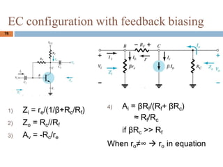
- 75. EC configuration with feedback biasing 76 1) Zi = re/(1/¦Â+Rc/Rf) 2) Zo = Rc//Rf 3) Av = -Rc/re 4) Ai = ¦ÂRf/(Rf+ ¦ÂRc) ˇÖ Rf/Rc if ¦ÂRc >> Rf When roˇŮˇŢ ˇú ro in equation
- 76. EC configuration with feedback biasing 77
- 77. 78 EC configuration with feedback biasing
- 78. 79 EC configuration with feedback biasing
- 79. 80 Analyze BC AC analysis methods rE model
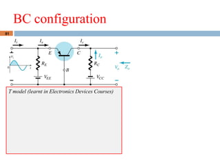
- 80. 81 BC configuration T model (learnt in Electronics Devices Courses)
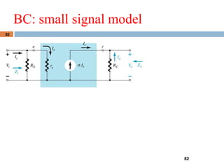
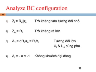
- 81. 82 BC: small signal model 82
- 84. 85 Analyze BC configuration 85 1) Zi = Re||re Tr? kh¨˘ng v¨¤o t??ng ??i nh? 2) Zo = Rc Tr? kh¨˘ng ra l?n 3) Av = ¦ÁRc/re ˇÖ Rc/re T??ng ??i l?n Ui & Uo c¨´ng pha 4) Ai = - ¦Á ˇÖ -1 Kh?ng khu?ch ??i d¨°ng
- 85. 86 Analyze CC
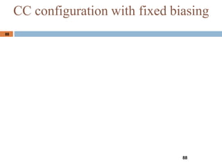
- 86. 87 87 CC configuration with fixed biasing
- 87. 88 CC configuration with fixed biasing 88
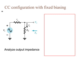
- 88. CC configuration with fixed biasing Analyze output impedance 89
- 89. Vo 90 CC configuration with fixed biasing
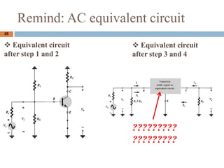
- 90. 1) Zi = Rb || [¦Âre+(¦Â+1)Re] ˇÖ Rb || ¦Â(re+Re) High input impedance 2) Zo = Re||re ˇÖ re where Re >> re Low output impedance 3) Av = Re/(Re+re) ˇÖ 1 Inphase with input and smaller amplitude => ˇ°emitter connectionˇ± 4) Ai = - ¦ÂRb/[Rb+ ¦Â(re+Re)] Application: Buffer 91 CC configuration with fixed biasing
- 91. Quizz ? 1. eq/. Circuit ? 2. Av; Ai 92
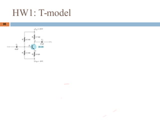
- 92. Homework 1: Determine Ai, Av, Zi, Zo? 93
- 93. Homework 1: 94
- 94. HW1: T-model 95
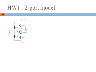
- 95. HW1 : 2-port model 96
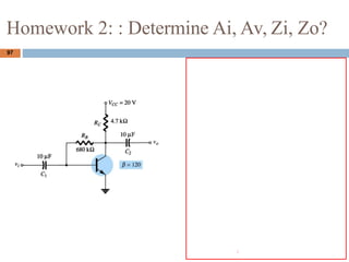
- 96. 97 Homework 2: : Determine Ai, Av, Zi, Zo?
- 97. 98
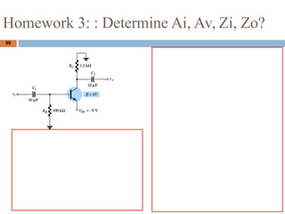
- 98. 99 Homework 3: : Determine Ai, Av, Zi, Zo?
- 99. Homework 3 100
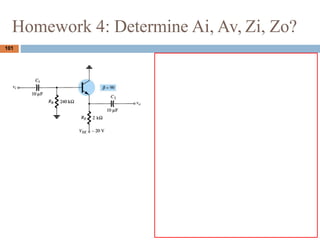
- 100. 101 Homework 4: Determine Ai, Av, Zi, Zo?
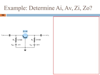
- 101. 102 Example: Determine Ai, Av, Zi, Zo?
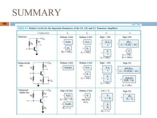
- 102. SUMMARY 103
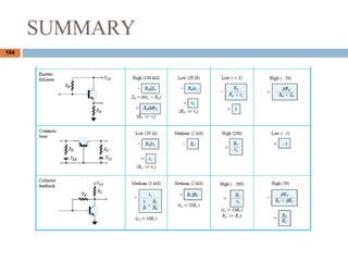
- 103. 104 SUMMARY
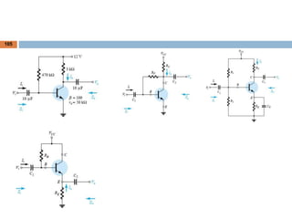
- 104. 105
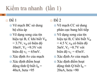
- 105. 106 Ki?m tra nhanh (l?n 1) ? ?? 1 ? V? m?ch BC s? dung b? chia ¨˘p ? V? d?ng song c?a t¨Şn hi?u t?i B, C khi bi?t VB = 3.7V, vB c¨® bi¨şn ?? 10mV, VC =9.3V v?i bi¨şn ?? vC = 65mV. ? X¨˘c ??nh Av c?a m?ch ? X¨˘c ??nh ?i?m ho?t ??ng t?nh Q bi?t IB = 40uA, beta =95 ? ?? 2 ? V? m?ch CC s? dung ph?n c?c bang h?i ti?p ? V? d?ng song c?a t¨Şn hi?u t?i B, C khi bi?t VB = 4.5 V, vB c¨® bi¨şn ?? 5mV, VC =8.7V v?i bi¨şn ?? vC = 45mV. ? X¨˘c ??nh Av c?a m?ch ? X¨˘c ??nh ?i?m ho?t ??ng t?nh Q bi?t IB = 20uA, beta =90