555 timer lab projects
- 1. Lab: 555 Timer Part I: Objective The purposes of this lab is to introduce students to construct a clock source using a 555 timer and study the importance of using buffer at the output of logic devices. Part II: Equipment List Tektronix 2225 Analog Oscilloscope / HP 54502A Digital Oscilloscope Tektronix P6103 10X probe / HP 10430A 10X probe Resistors Capacitors DC Power Supply Breadboard 555 Timer chip, NAND gates, Inverter gates.
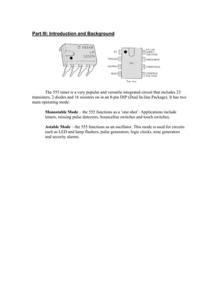
- 2. Part III: Introduction and Background The 555 timer is a very popular and versatile integrated circuit that includes 23 transisters, 2 diodes and 16 resisters on in an 8-pin DIP (Dual In-line Package). It has two main operating mode: Monostable Mode – the 555 functions as a ‘one-shot’. Applications include timers, missing pulse detectors, bouncefree switches and touch switches. Astable Mode – the 555 functions as an oscillator. This mode is used for circuits such as LED and lamp flashers, pulse generators, logic clocks, tone generators and security alarms.
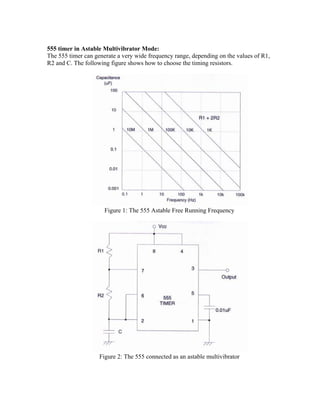
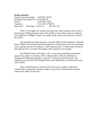
- 3. 555 timer in Astable Multivibrator Mode: The 555 timer can generate a very wide frequency range, depending on the values of R1, R2 and C. The following figure shows how to choose the timing resistors. Figure 1: The 555 Astable Free Running Frequency Figure 2: The 555 connected as an astable multivibrator
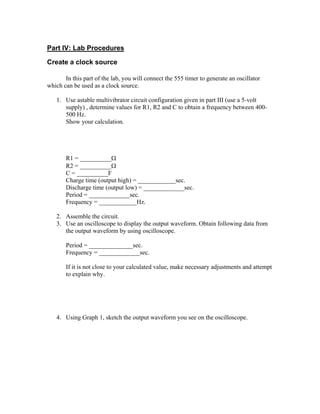
- 4. Design equations: Charge time (output high): 0.693*(R1+R2)*C Discharge time (output low): 0.693*(R2)*C Period: 0.693*(R1+2*R2) Frequency: 1.44 / ((R1+2*R2)*C) Duty cycle: Time High / Time Low: (R1+R2) / R2 With a 5-volt supply, the resistors can range from 1KΩ (minimum value of R1 or R2) through 3.3MΩ (maximum value of R1 and R2 in series). Best results are obtained with capacitors of 1000pF or larger, but smaller values can be used with lower values of R1 and R2. The maximum operating frequency is around 1Mhz, but best operation is obtained below 300kHz. The minimum operating frequency is limited only by the size and leakage of the capacitor you use. For instance, a 10µF capacitor and a 3.3 MΩ resistor will give a time interval of 23.1 seconds if the leakage of the capacitor is low enough. By making R2 large with respect to R1, we can get an essentially symmetrical square-wave output. For instance, if R1 is 1KΩ and R2 is 1MΩ, the difference in charging and discharging resistance is only 0.1%, and good symmetry results. Any symmetry you want from 50% through 99.9% can be obtained by a selection of the ratio of R1 and R2. Only a small frequency variation occurs due to power supply variation but variation due to temperature changes is large, so any precise instrumentation projects require more stable crystal clock.
- 5. Part IV: Lab Procedures Create a clock source In this part of the lab, you will connect the 555 timer to generate an oscillator which can be used as a clock source. 1. Use astable multivibrator circuit configuration given in part III (use a 5-volt supply) , determine values for R1, R2 and C to obtain a frequency between 400- 500 Hz. Show your calculation. R1 = __________Ω R2 = __________Ω C = __________F Charge time (output high) = ____________sec. Discharge time (output low) = _____________sec. Period = _____________sec. Frequency = ____________Hz. 2. Assemble the circuit. 3. Use an oscilloscope to display the output waveform. Obtain following data from the output waveform by using oscilloscope. Period = ______________sec. Frequency = _____________sec. If it is not close to your calculated value, make necessary adjustments and attempt to explain why. 4. Using Graph 1, sketch the output waveform you see on the oscilloscope.
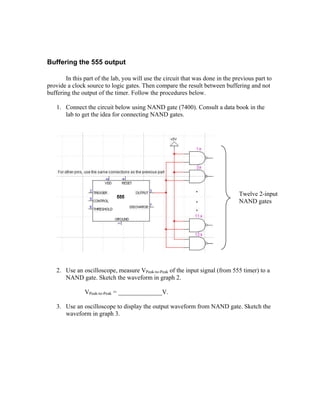
- 6. Buffering the 555 output In this part of the lab, you will use the circuit that was done in the previous part to provide a clock source to logic gates. Then compare the result between buffering and not buffering the output of the timer. Follow the procedures below. 1. Connect the circuit below using NAND gate (7400). Consult a data book in the lab to get the idea for connecting NAND gates. Twelve 2-input NAND gates 2. Use an oscilloscope, measure VPeak-to-Peak of the input signal (from 555 timer) to a NAND gate. Sketch the waveform in graph 2. VPeak-to-Peak = ______________V. 3. Use an oscilloscope to display the output waveform from NAND gate. Sketch the waveform in graph 3.
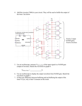
- 7. 4. Add Hex inverter (7404) to your circuit. They will be used to buffer the output of the timer. See below Twelve 2-input NAND gates, Twelve inverters 5. Use an oscilloscope, measure VPeak-to-Peak of the input signal to a NAND gate (output of inverter). Sketch the waveform in graph 4. VPeak-to-Peak = ______________V. 6. Use an oscilloscope to display the output waveform from NAND gate. Sketch the waveform in graph 5. 7. Is there any difference between buffering and not buffering the output of the timer? If yes, why is that? Comment on the result.
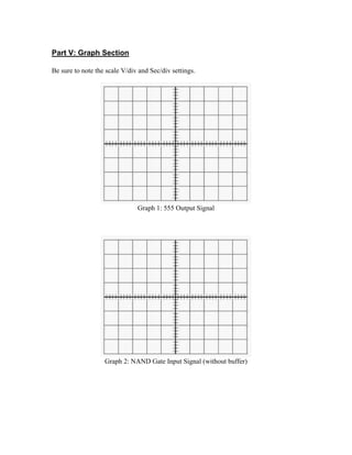
- 8. Part V: Graph Section Be sure to note the scale V/div and Sec/div settings. Graph 1: 555 Output Signal Graph 2: NAND Gate Input Signal (without buffer)
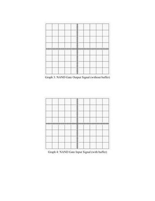
- 9. Graph 3: NAND Gate Output Signal (without buffer) Graph 4: NAND Gate Input Signal (with buffer)
- 10. Graph 5: NAND Gate Output Signal (with buffer)


