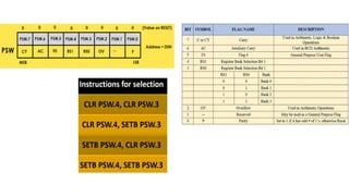
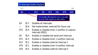
![LCD Interfacing with 8051 Microcontroller
LCD Interfacing Module Review
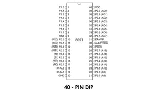
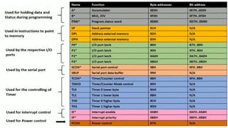
16Ã2 LCD module is a very common type of LCD module to be used in 8051 based embedded projects. It has 16 rows
and 2 columns [5Ã7] or [5Ã8] LCD dot matrices. Available in 16 pin packages with features like contrast adjustment
function, backlight, and each dot matrix has 5Ã8 dot resolution. The PINs, their name and functions are shown in the
table below.](https://image.slidesharecdn.com/8051-220921172641-8060f2dd/85/8051-pdf-105-320.jpg)

8051.pdf
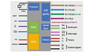
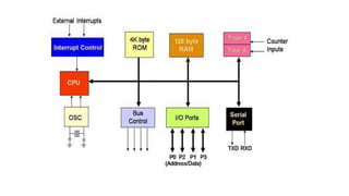
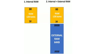
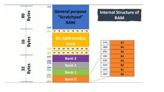
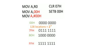
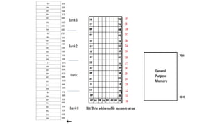
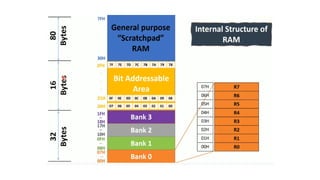
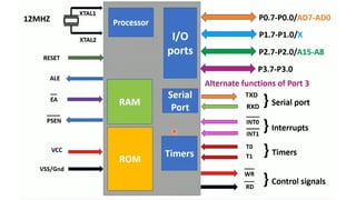
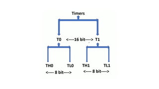
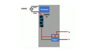
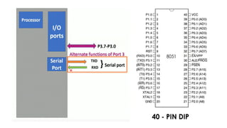
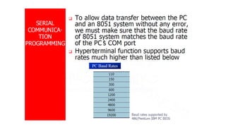
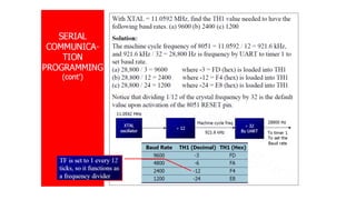
- 3. 8051 Microcontroller Features âĒ8 â Bit ALU: ALU or Arithmetic Logic Unit is the heart of a microcontroller. It performs arithmetic and bitwise operation on binary numbers. The ALU in 8051 is an 8 â Bit ALU i.e. it can perform operations on 8 â bit data. âĒ8 â Bit Accumulator:The Accumulator is an important register associated with the ALU. The accumulator in 8051 is an 8 â bit register. âĒRAM: 8051 Microcontroller has 128 Bytes of RAM which includes SFRs and Input / Output Port Registers. âĒROM: 8051 has 4 KB of on-chip ROM (Program Memory). âĒI/O Ports: 8051 has four 8 â bit Input / Output Ports which are bit addressable and bidirectional. âĒTimers / Counters: 8051 has two 16 â bit Timers / Counters. âĒSerial Port: 8051 supports full duplex UART Communication. âĒExternal Memory: 8051Microcontroller can access two 16 â bit address line at once: one each for RAM and ROM. The total external memory that an 8051 Microcontroller can access for RAM and ROM is 64KB (216 for each type). âĒAdditional Features: Interrupts, on-chip oscillator, Boolean Processor.
- 4. Applications of 8051 Microcontroller âĒConsumer Appliances (TV Tuners, Remote controls, Computers, Sewing Machines, etc.) âĒHome Applications (TVs, VCR, Video Games, Camcorder, Music Instruments, Home Security Systems, Garage Door Openers, etc.) âĒCommunication Systems (Mobile Phones, Intercoms, Answering Machines, Paging Devices, etc.) âĒOffice (Fax Machines, Printers, Copiers, Laser Printers, etc.) âĒAutomobiles (Air Bags, ABS, Engine Control, Transmission Control, Temperature Control, Keyless Entry, etc) âĒAeronautical and Space âĒMedical Equipment âĒDefense Systems âĒRobotics
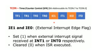
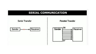
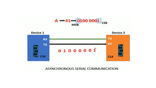
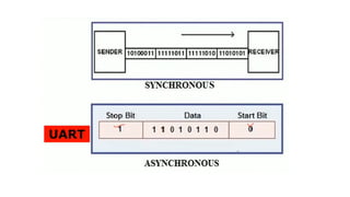
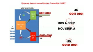
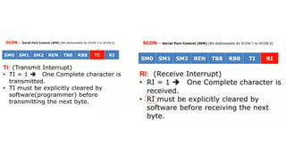
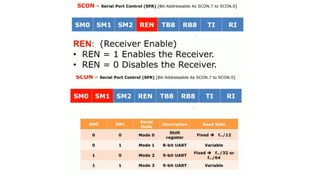
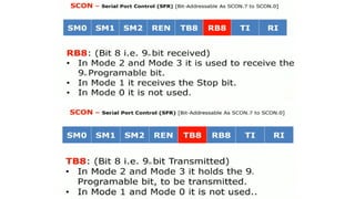
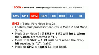
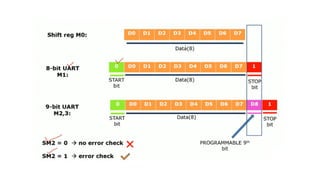
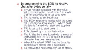
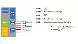
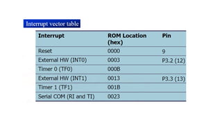
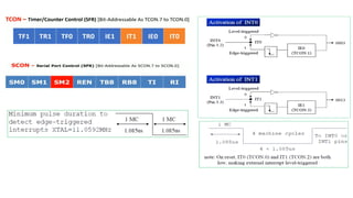
- 71. Universal Asynchronous Receiver Transmitter (UART)
- 105. LCD Interfacing with 8051 Microcontroller LCD Interfacing Module Review 16Ã2 LCD module is a very common type of LCD module to be used in 8051 based embedded projects. It has 16 rows and 2 columns [5Ã7] or [5Ã8] LCD dot matrices. Available in 16 pin packages with features like contrast adjustment function, backlight, and each dot matrix has 5Ã8 dot resolution. The PINs, their name and functions are shown in the table below.
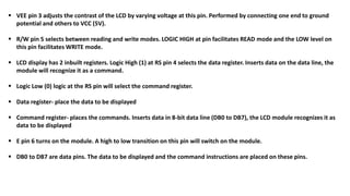
- 106. ⊠VEE pin 3 adjusts the contrast of the LCD by varying voltage at this pin. Performed by connecting one end to ground potential and others to VCC (5V). ⊠R/W pin 5 selects between reading and write modes. LOGIC HIGH at pin facilitates READ mode and the LOW level on this pin facilitates WRITE mode. ⊠LCD display has 2 inbuilt registers. Logic High (1) at RS pin 4 selects the data register. Inserts data on the data line, the module will recognize it as a command. ⊠Logic Low (0) logic at the RS pin will select the command register. ⊠Data register- place the data to be displayed ⊠Command register- places the commands. Inserts data in 8-bit data line (DB0 to DB7), the LCD module recognizes it as data to be displayed ⊠E pin 6 turns on the module. A high to low transition on this pin will switch on the module. ⊠DB0 to DB7 are data pins. The data to be displayed and the command instructions are placed on these pins.
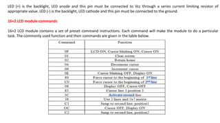
- 107. LED (+) is the backlight, LED anode and this pin must be connected to Vcc through a series current limiting resistor of appropriate value. LED (-) is the backlight, LED cathode and this pin must be connected to the ground. 16Ã2 LCD module commands 16Ã2 LCD module contains a set of preset command instructions. Each command will make the module to do a particular task. The commonly used function and their commands are given in the table below.
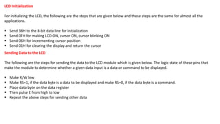
- 108. LCD Initialization For initializing the LCD, the following are the steps that are given below and these steps are the same for almost all the applications. ⊠Send 38H to the 8-bit data line for initialization ⊠Send 0FH for making LCD ON, cursor ON, cursor blinking ON ⊠Send 06H for incrementing cursor position ⊠Send 01H for clearing the display and return the cursor Sending Data to the LCD The following are the steps for sending the data to the LCD module which is given below. The logic state of these pins that make the module to determine whether a given data input is a data or command to be displayed. ⊠Make R/W low ⊠Make RS=1, if the data byte is a data to be displayed and make RS=0, if the data byte is a command. ⊠Place data byte on the data register ⊠Then pulse E from high to low ⊠Repeat the above steps for sending other data
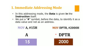
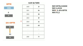
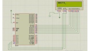
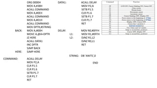
- 110. ORG 0000H MOV A,#38H ACALL COMMAND MOV A,#0EH ACALL COMMAND MOV A,#01H ACALL COMMAND MOV DPTR,#STRING BACK: MOV A,#00H MOVC A,@A+DPTR JZ HERE ACALL DATA1 INC DPTR SJMP BACK HERE: SJMP HERE COMMAND: ACALL DELAY MOV P2,A CLR P1.5 CLR P1.6 SETB P1.7 CLR P1.7 RET DATA1: ACALL DELAY MOV P2,A SETB P1.5 CLR P1.6 SETB P1.7 CLR P1.7 RET DELAY: MOV R0,#0FFH L1: MOV R1,#0FFH L2: DJNZ R1,L2 DJNZ R0,L1 RET STRING: DB 'ANITS',0 END
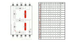
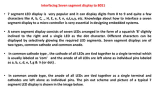
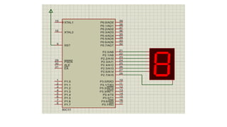
- 111. Interfacing Seven segment display to 8051 âĒ 7 segment LED display is very popular and it can display digits from 0 to 9 and quite a few characters like A, b, C, ., H, E, e, F, n, o,t,u,y, etc. Knowledge about how to interface a seven segment display to a micro controller is very essential in designing embedded systems. âĒ A seven segment display consists of seven LEDs arranged in the form of a squarish â8â slightly inclined to the right and a single LED as the dot character. Different characters can be displayed by selectively glowing the required LED segments. Seven segment displays are of two types, common cathode and common anode. âĒ In common cathode type , the cathode of all LEDs are tied together to a single terminal which is usually labeled as âcomâ and the anode of all LEDs are left alone as individual pins labeled as a, b, c, d, e, f, g & h (or dot) . âĒ In common anode type, the anode of all LEDs are tied together as a single terminal and cathodes are left alone as individual pins. The pin out scheme and picture of a typical 7 segment LED display is shown in the image below.
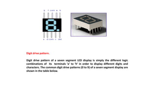
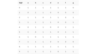
- 112. Digit drive pattern. Digit drive pattern of a seven segment LED display is simply the different logic combinations of its terminals âaâ to âhâ in order to display different digits and characters. The common digit drive patterns (0 to 9) of a seven segment display are shown in the table below.
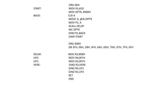
- 115. ORG 00H START: MOV R1,#10 MOV DPTR, #400H BACK: CLR A MOVC A, @A+DPTR MOV P2, A ACALL DELAY INC DPTR DJNZ R1,BACK SJMP START ORG 400H DB 3FH, 06H, 5BH, 4FH, 66H, 6DH, 7DH, 07H, 7FH, 6FH DELAY: MOV R2,#08H UP2: MOV R4,0FFH UP1: MOV R3,0FFH HERE: DJNZ R3,HERE DJNZ R4,UP1 DJNZ R2,UP2 RET END
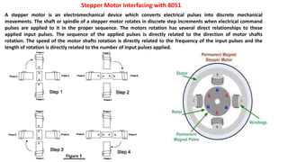
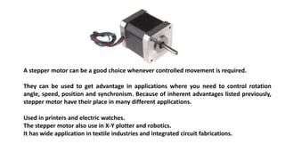
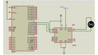
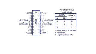
- 116. Stepper Motor Interfacing with 8051 A stepper motor is an electromechanical device which converts electrical pulses into discrete mechanical movements. The shaft or spindle of a stepper motor rotates in discrete step increments when electrical command pulses are applied to it in the proper sequence. The motors rotation has several direct relationships to these applied input pulses. The sequence of the applied pulses is directly related to the direction of motor shafts rotation. The speed of the motor shafts rotation is directly related to the frequency of the input pulses and the length of rotation is directly related to the number of input pulses applied.
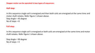
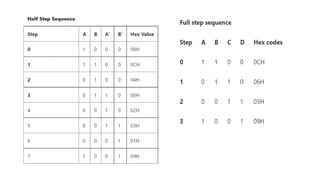
- 117. Stepper motor can be operated in two types of sequences: Half step: In this sequence single coil is energized and then both coils are energized at the same time and motor shaft rotates. Refer figure 1 shown above. Step Angle = 45 degree No of steps = 8 Full step: In this sequence single coil is energized or both coils are energized at the same time and motor shaft rotates. Refer figure 1 shown above. Step Angle = 90 degree No of steps = 4
- 119. A stepper motor can be a good choice whenever controlled movement is required. They can be used to get advantage in applications where you need to control rotation angle, speed, position and synchronism. Because of inherent advantages listed previously, stepper motor have their place in many different applications. Used in printers and electric watches. The stepper motor also use in X-Y plotter and robotics. It has wide application in textile industries and integrated circuit fabrications.
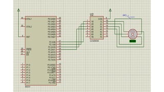
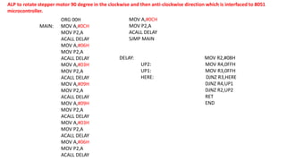
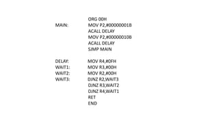
- 121. ALP to rotate stepper motor 90 degree in the clockwise and then anti-clockwise direction which is interfaced to 8051 microcontroller. ORG 00H MAIN: MOV A,#0CH MOV P2,A ACALL DELAY MOV A,#06H MOV P2,A ACALL DELAY MOV A,#03H MOV P2,A ACALL DELAY MOV A,#09H MOV P2,A ACALL DELAY MOV A,#09H MOV P2,A ACALL DELAY MOV A,#03H MOV P2,A ACALL DELAY MOV A,#06H MOV P2,A ACALL DELAY DELAY: MOV R2,#08H UP2: MOV R4,0FFH UP1: MOV R3,0FFH HERE: DJNZ R3,HERE DJNZ R4,UP1 DJNZ R2,UP2 RET END MOV A,#0CH MOV P2,A ACALL DELAY SJMP MAIN
- 124. ORG 00H MAIN: MOV P2,#00000001B ACALL DELAY MOV P2,#00000010B ACALL DELAY SJMP MAIN DELAY: MOV R4,#0FH WAIT1: MOV R3,#00H WAIT2: MOV R2,#00H WAIT3: DJNZ R2,WAIT3 DJNZ R3,WAIT2 DJNZ R4,WAIT1 RET END
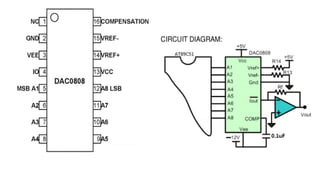
- 125. Digital to Analog Converter (DAC) Interfacing with 8051 microcontroller
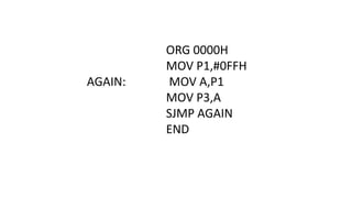
- 130. ORG 0000H MOV P1,#0FFH AGAIN: MOV A,P1 MOV P3,A SJMP AGAIN END
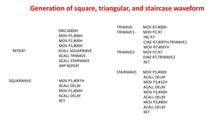
- 131. ORG 0000H MOV P1,#00H MOV P2,#00H MOV P3,#00H REPEAT: ACALL SQUARWAVE ACALL TRIWAVE ACALL STAIRWAVE JMP REPEAT SQUARWAVE: MOV P1,#0FFH ACALL DELAY MOV P1,#00H ACALL DELAY RET TRIWAVE: MOV R7,#00H TRIWAVE1: MOV P2,R7 INC R7 CJNE R7,#0FFH,TRIWAVE1 MOV R7,#0FFH TRIWAVE2: MOV P2,R7 DJNZ R7,TRIWAVE2 RET STAIRWAVE: MOV P3,#00H ACALL DELAY MOV P3,#32H ACALL DELAY MOV P3,#40H ACALL DELAY MOV P3,#80H ACALL DELAY RET Generation of square, triangular, and staircase waveform
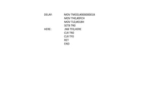
- 132. DELAY: MOV TMOD,#00000001B MOV TH0,#0FCH MOV TL0,#018H SETB TR0 HERE: JNB TF0,HERE CLR TR0 CLR TF0 RET END
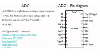
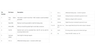
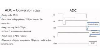
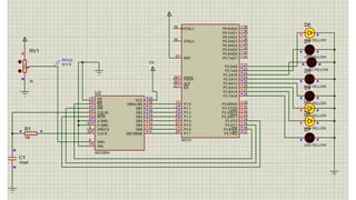
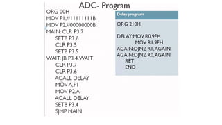
- 133. Analog to digital Converter (ADC) Interfacing with 8051 microcontroller
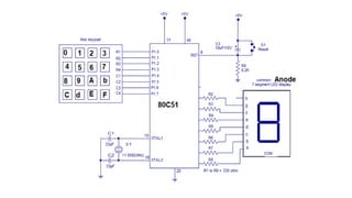
- 139. 4X4 Keypad Interfacing with 8051 Microcontroller
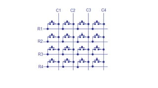
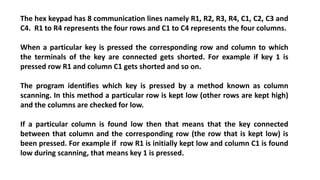
- 142. The hex keypad has 8 communication lines namely R1, R2, R3, R4, C1, C2, C3 and C4. R1 to R4 represents the four rows and C1 to C4 represents the four columns. When a particular key is pressed the corresponding row and column to which the terminals of the key are connected gets shorted. For example if key 1 is pressed row R1 and column C1 gets shorted and so on. The program identifies which key is pressed by a method known as column scanning. In this method a particular row is kept low (other rows are kept high) and the columns are checked for low. If a particular column is found low then that means that the key connected between that column and the corresponding row (the row that is kept low) is been pressed. For example if row R1 is initially kept low and column C1 is found low during scanning, that means key 1 is pressed.
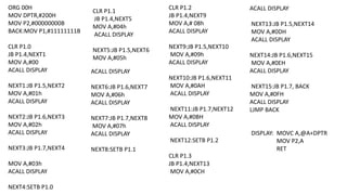
- 143. ORG 00H MOV DPTR,#200H MOV P2,#00000000B BACK:MOV P1,#11111111B CLR P1.0 JB P1.4,NEXT1 MOV A,#00 ACALL DISPLAY NEXT1:JB P1.5,NEXT2 MOV A,#01h ACALL DISPLAY NEXT2:JB P1.6,NEXT3 MOV A,#02h ACALL DISPLAY NEXT3:JB P1.7,NEXT4 MOV A,#03h ACALL DISPLAY NEXT4:SETB P1.0 CLR P1.1 JB P1.4,NEXT5 MOV A,#04h ACALL DISPLAY NEXT5:JB P1.5,NEXT6 MOV A,#05h ACALL DISPLAY NEXT6:JB P1.6,NEXT7 MOV A,#06h ACALL DISPLAY NEXT7:JB P1.7,NEXT8 MOV A,#07h ACALL DISPLAY NEXT8:SETB P1.1 CLR P1.2 JB P1.4,NEXT9 MOV A,# 08h ACALL DISPLAY NEXT9:JB P1.5,NEXT10 MOV A,#09h ACALL DISPLAY NEXT10:JB P1.6,NEXT11 MOV A,#0AH ACALL DISPLAY NEXT11:JB P1.7,NEXT12 MOV A,#0BH ACALL DISPLAY NEXT12:SETB P1.2 CLR P1.3 JB P1.4,NEXT13 MOV A,#0CH ACALL DISPLAY NEXT13:JB P1.5,NEXT14 MOV A,#0DH ACALL DISPLAY NEXT14:JB P1.6,NEXT15 MOV A,#0EH ACALL DISPLAY NEXT15:JB P1.7, BACK MOV A,#0FH ACALL DISPLAY LJMP BACK DISPLAY: MOVC A,@A+DPTR MOV P2,A RET
- 144. ORG 200H DB 11000000B DB 11111001B DB 10100100B DB 10110000B DB 10011001B DB 10010010B DB 10000010B DB 11111000B DB 10000000B DB 10010000B DB 10001000B DB 10000011B DB 11000110B DB 10100001B DB 10000110B DB 10001110B END
- 145. Memory Interfacing with 8051 Microcontroller
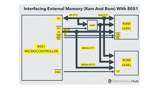
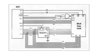
- 148. Step 1: Connect RD to OE of ext. RAM. Step 2: Connect WR to WE of ext. RAM. Step 3: Connect active low input of NAND gate to CE of external RAM
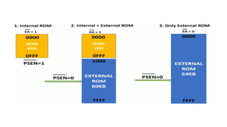
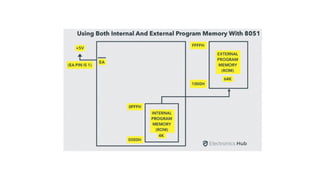
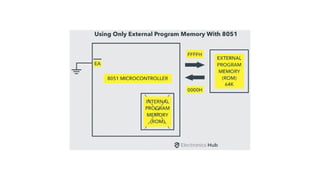
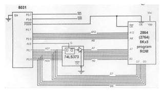
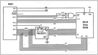
- 150. Step 1: Connect EA pin to ground Step 2: Connect the PSEN to the CE and OE. Step 3: Then, Port 2 (P2.0 â P2.7) to A8 â A12 pins of ext. ROM. Step 4: Connect ALE to G of 74LS373 latch to enable it. Step 5: Next, connect the OC of 74LS373 to GND. Step 6: Connect Port 0 (P0.0 â P0.7), which consists of both address and data multiplexed into Port 0 to 1D â 8D pins of 74LS373 latch to demultiplex it and 1Q â 8Q of the latch to A0 â A7 of ext. ROM. Step 7: Connect Port 0 (P0.0 â P0.7) to D0 â D7 of the ext. ROM. Step 8: VPP of ext. ROM to VCC.