際際滷

際際滷Share a Scribd company logo
DM74LS90 Decade and Binary Counters
                                                                                                                      August 1986
                                                                                                                      Revised March 2000


 DM74LS90
 Decade and Binary Counters
 General Description                                                               Features
 Each of these monolithic counters contains four master-                           s Typical power dissipation 45 mW
 slave flip-flops and additional gating to provide a divide-by-                    s Count frequency 42 MHz
 two counter and a three-stage binary counter for which the
 count cycle length is divide-by-five for the DM74LS90.
 All of these counters have a gated zero reset and the
 DM74LS90 also has gated set-to-nine inputs for use in
 BCD nines complement applications.
 To use their maximum count length (decade or four bit
 binary), the B input is connected to the QA output. The
 input count pulses are applied to input A and the outputs
 are as described in the appropriate truth table. A symmetri-
 cal divide-by-ten count can be obtained from the
 DM74LS90 counters by connecting the QD output to the A
 input and applying the input count to the B input which
 gives a divide-by-ten square wave at output QA.


 Ordering Code:
  Order Number           Package Number                                                     Package Description
DM74LS90M                        M14A              14-Lead Small Outline Integrated Circuit (SOIC), JEDEC MS-120, 0.150 Narrow
DM74LS90N                        N14A              14-Lead Plastic Dual-In-Line Package (PDIP), JEDEC MS-001, 0.300 Wide
 Devices also available in Tape and Reel. Specify by appending the suffix letter X to the ordering code.


 Connection Diagram                                                                Reset/Count Truth Table
                                                                                                  Reset Inputs                      Output
                                                                                      R0(1)      R0(2)       R9(1)   R9(2)   QD     QC   QB   QA
                                                                                        H           H         L       X      L      L    L    L
                                                                                        H           H         X       L      L      L    L    L
                                                                                        X           X         H       H      H      L    L    H
                                                                                        X           L         X       L             COUNT
                                                                                        L           X         L       X             COUNT
                                                                                        L           X         X       L             COUNT
                                                                                        X           L         L       X             COUNT


息 2000 Fairchild Semiconductor Corporation                    DS006381                                                       www.fairchildsemi.com
DM74LS90
            Function Tables                                                            Logic Diagram
                                   BCD Count Sequence (Note 1)

                 Count                                   Output
                                    QD            QC              QB          QA
                     0               L              L             L           L
                     1               L              L             L           H
                     2               L              L             H           L
                     3               L              L             H           H
                     4               L             H              L           L
                     5               L             H              L           H
                     6               L             H              H           L
                     7               L             H              H           H
                     8               H              L             L           L
                     9               H              L             L           H

                                      Bi-Quinary (5-2) (Note 2)

                 Count                                   Output
                                    QA            QD              QC          QB
                     0               L              L             L           L
                     1               L              L             L           H
                     2               L              L             H           L
                     3               L              L             H           H
                     4               L             H              L           L
                     5               H              L             L           L
                     6               H              L             L           H
                     7               H              L             H           L
                     8               H              L             H           H
                     9               H             H              L           L

            H = HIGH Level
            L = LOW Level
            X = Dont Care
            Note 1: Output QA is connected to input B for BCD count.                   The J and K inputs shown without connection are for reference only and
                                                                                       are functionally at a high level.
            Note 2: Output QD is connected to input A for bi-quinary count.

            Note 3: Output QA is connected to input B.


           www.fairchildsemi.com                                                   2
DM74LS90
 Absolute Maximum Ratings(Note 4)
 Supply Voltage                                                            7V
                                                                                    Note 4: The Absolute Maximum Ratings are those values beyond which
 Input Voltage (Reset)                                                     7V       the safety of the device cannot be guaranteed. The device should not be
                                                                                    operated at these limits. The parametric values defined in the Electrical
 Input Voltage (A or B)                                               5.5V          Characteristics table are not guaranteed at the absolute maximum ratings.
 Operating Free Air Temperature Range                       0属C to +70属C            The Recommended Operating Conditions table will define the conditions
                                                                                    for actual device operation.
 Storage Temperature Range                              65属C to +150属C


 Recommended Operating Conditions
      Symbol                                  Parameter                                        Min               Nom                Max              Units
VCC                  Supply Voltage                                                            4.75                 5               5.25               V
VIH                  HIGH Level Input Voltage                                                    2                                                     V
VIL                  LOW Level Input Voltage                                                                                        0.8                V
IOH                  HIGH Level Output Current                                                                                      0.4              mA
IOL                  LOW Level Output Current                                                                                        8                mA
fCLK                 Clock Frequency (Note 5)                    A to QA                         0                                   32              MHz
                                                                 B to QB                         0                                   16
fCLK                 Clock Frequency (Note 6)                    A to QA                         0                                   20              MHz
                                                                 B to QB                         0                                   10
tW                   Pulse Width (Note 5)                        A                              15
                                                                 B                              30                                                     ns
                                                                 Reset                          15
tW                   Pulse Width (Note 6)                        A                              25
                                                                 B                              50                                                     ns
                                                                 Reset                          25
tREL                 Reset Release Time (Note 5)                                                25                                                     ns
tREL                 Reset Release Time (Note 6)                                                35                                                     ns
TA                   Free Air Operating Temperature                                              0                                   70                属C
 Note 5: CL = 15 pF, RL = 2 k, TA = 25属C and VCC = 5V.
 Note 6: CL = 50 pF, RL = 2 k, TA = 25属C and VCC = 5V.


 Electrical Characteristics
 over recommended operating free air temperature range (unless otherwise noted)
                                                                                                                            Typ
     Symbol               Parameter                                  Conditions                               Min                          Max         Units
                                                                                                                         (Note 7)
VI            Input Clamp Voltage                   VCC = Min, II = 18 mA                                                                 1.5            V
VOH           HIGH Level                            VCC = Min, IOH = Max
                                                                                                              2.7           3.4                            V
              Output Voltage                        VIL = Max, VIH = Min
VOL           LOW Level                             VCC = Min, IOL = Max
                                                                                           (Note 8)
              Output Voltage                        VIL = Max, VIH = Min                                                    0.35           0.5             V
                                                    IOL = 4 mA, VCC = Min                                                   0.25           0.4
II            Input Current @ Max                   VCC = Max, VI = 7V                     Reset                                           0.1
              Input Voltage                         VCC = Max                              A                                               0.2           mA
                                                    VI = 5.5V                              B                                               0.4
IIH           HIGH Level                            VCC = Max, VI = 2.7V                   Reset                                            20
              Input Current                                                                A                                                40           袖A
                                                                                           B                                                80
IIL           LOW Level                             VCC = Max, VI = 0.4V                   Reset                                           0.4
              Input Current                                                                A                                               2.4          mA
                                                                                           B                                               3.2
IOS           Short Circuit Output Current          VCC = Max (Note 9)                                        20                          100          mA
ICC           Supply Current                        VCC = Max (Note 7)                                                       9              15           mA
 Note 7: All typicals are at VCC = 5V, TA = 25属C.


                                                                                3                                                    www.fairchildsemi.com
DM74LS90
            Electrical Characteristics                                 (Continued)
            Note 8: QA outputs are tested at IOL = Max plus the limit value of IIL for the B input. This permits driving the B input while maintaining full fan-out capability.
            Note 9: Not more than one output should be shorted at a time, and the duration should not exceed one second.
            Note 10: ICC is measured with all outputs open, both RO inputs grounded following momentary connection to 4.5V and all other inputs grounded.


            Switching Characteristics at VCC = 5V and TA = 25属C
                                                                               From (Input)                                        RL = 2 k
             Symbol                     Parameter                              To (Output)                       CL = 15 pF                     CL = 50 pF                Units
                                                                                                              Min            Max            Min            Max
           fMAX           Maximum Clock                                           A to QA                     32                               20
                                                                                                                                                                          MHz
                          Frequency                                               B to QB                     16                               10
           tPLH           Propagation Delay Time
                                                                                  A to QA                                     16                            20             ns
                          LOW-to-HIGH Level Output
           tPHL           Propagation Delay Time
                                                                                  A to QA                                     18                            24             ns
                          HIGH-to-LOW Level Output
           tPLH           Propagation Delay Time
                                                                                  A to QD                                     48                            52             ns
                          LOW-to-HIGH Level Output
           tPHL           Propagation Delay Time
                                                                                  A to QD                                     50                            60             ns
                          HIGH-to-LOW Level Output
           tPLH           Propagation Delay Time
                                                                                  B to QB                                     16                            23             ns
                          LOW-to-HIGH Level Output
           tPHL           Propagation Delay Time
                                                                                  B to QB                                     21                            30             ns
                          HIGH-to-LOW Level Output
           tPLH           Propagation Delay Time
                                                                                  B to QC                                     32                            37             ns
                          LOW-to-HIGH Level Output
           tPHL           Propagation Delay Time
                                                                                  B to QC                                     35                            44             ns
                          HIGH-to-LOW Level Output
           tPLH           Propagation Delay Time
                                                                                  B to QD                                     32                            36             ns
                          LOW-to-HIGH Level Output
           tPHL           Propagation Delay Time
                                                                                  B to QD                                     35                            44             ns
                          HIGH-to-LOW Level Output
           tPLH           Propagation Delay Time
                                                                             SET-9 to QA, QD                                  30                            35             ns
                          LOW-to-HIGH Level Output
           tPHL           Propagation Delay Time
                                                                             SET-9 to QB, QC                                  40                            48             ns
                          HIGH-to-LOW Level Output
           tPHL           Propagation Delay Time
                                                                             SET-0 to Any Q                                   40                            52             ns
                          HIGH-to-LOW Level Output


           www.fairchildsemi.com                                                              4
DM74LS90
Physical Dimensions inches (millimeters) unless otherwise noted


               14-Lead Small Outline Integrated Circuit (SOIC), JEDEC MS-120, 0.150 Narrow
                                          Package Number M14A


                                                    5                                        www.fairchildsemi.com
DM74LS90 Decade and Binary Counters
                                       Physical Dimensions inches (millimeters) unless otherwise noted (Continued)


                                                              14-Lead Plastic Dual-In-Line Package (PDIP), JEDEC MS-001, 0.300 Wide
                                                                                       Package Number N14A


                                       Fairchild does not assume any responsibility for use of any circuitry described, no circuit patent licenses are implied and
                                       Fairchild reserves the right at any time without notice to change said circuitry and specifications.
                                       LIFE SUPPORT POLICY

                                       FAIRCHILDS PRODUCTS ARE NOT AUTHORIZED FOR USE AS CRITICAL COMPONENTS IN LIFE SUPPORT
                                       DEVICES OR SYSTEMS WITHOUT THE EXPRESS WRITTEN APPROVAL OF THE PRESIDENT OF FAIRCHILD
                                       SEMICONDUCTOR CORPORATION. As used herein:
                                       1. Life support devices or systems are devices or systems            2. A critical component in any component of a life support
                                          which, (a) are intended for surgical implant into the                device or system whose failure to perform can be rea-
                                          body, or (b) support or sustain life, and (c) whose failure          sonably expected to cause the failure of the life support
                                          to perform when properly used in accordance with                     device or system, or to affect its safety or effectiveness.
                                          instructions for use provided in the labeling, can be rea-
                                          sonably expected to result in a significant injury to the                                            www.fairchildsemi.com
                                          user.

                                      www.fairchildsemi.com                                             6
This datasheet has been downloaded from:

      www.DatasheetCatalog.com

  Datasheets for electronic components.
Ad

Recommended

DataSheet 74ls90
DataSheet 74ls90
Carp_Diem
Microcontroller 8051 soft
baluusa8
Suzuki lecture-slides (1)
Ashok Kumar
Learn arduino hardware
Open.Embedded
Ejercicios capitulo3theveninynortonpro
Gabechan
Leslie
LeslieSanabria
Bachelor of commerce
QianJiadong
Info Tech Final Paper
Leonsagara
Watershapes Girona Spain
watershapes eu
Twitter Make Issue
Twitter Make Issue
Agenda King KeynaSee
犖犖迦牽犢犖犖ム厳犢犖犖犖幡犖朽犢犖犖犖犢犖迦犢
thanakit553
4 犖犖迦牽犢犖犖ム厳犢犖犖犖犖朽犢犖犖犖犢犖迦犢
topofzeed
04犖犖迦牽犢犖犖ム厳犢犖犖犖犖朽犢犖犖犖犢犖迦犢
Doc Edu
Multiplicador 3bits
Multiplicador 3bits
Vladimir Araujo
Calculo2lista1
Calculo2lista1
Cleide Soares
Girata gigli basso ( mano sinistra tastiera)
guest26abca
SPICE MODEL of TC74HC10AP in SPICE PARK
Tsuyoshi Horigome
Traffic signal-project-
Rajeev Verma
Tazkarti
Tazkarti
Mohamed Wagdy
Derecho Ingles
Derecho Ingles
mariainesfd
SPICE MODEL of TC74HCT08AF in SPICE PARK
Tsuyoshi Horigome
SPICE MODEL of TC74HCT08AFN in SPICE PARK
Tsuyoshi Horigome
SPICE MODEL of TC74VHC08F in SPICE PARK
Tsuyoshi Horigome
SPICE MODEL of TC74VHC08FN in SPICE PARK
Tsuyoshi Horigome
SPICE MODEL of TC74VHC08FT in SPICE PARK
Tsuyoshi Horigome
SPICE MODEL of TC74HCT08AP in SPICE PARK
Tsuyoshi Horigome
SPICE MODEL of TC74VHCT08AF in SPICE PARK
Tsuyoshi Horigome
SPICE MODEL of TC74HC08AF in SPICE PARK
Tsuyoshi Horigome

More Related Content

Similar to 90 (20)

Watershapes Girona Spain
watershapes eu
Twitter Make Issue
Twitter Make Issue
Agenda King KeynaSee
犖犖迦牽犢犖犖ム厳犢犖犖犖幡犖朽犢犖犖犖犢犖迦犢
thanakit553
4 犖犖迦牽犢犖犖ム厳犢犖犖犖犖朽犢犖犖犖犢犖迦犢
topofzeed
04犖犖迦牽犢犖犖ム厳犢犖犖犖犖朽犢犖犖犖犢犖迦犢
Doc Edu
Multiplicador 3bits
Multiplicador 3bits
Vladimir Araujo
Calculo2lista1
Calculo2lista1
Cleide Soares
Girata gigli basso ( mano sinistra tastiera)
guest26abca
SPICE MODEL of TC74HC10AP in SPICE PARK
Tsuyoshi Horigome
Traffic signal-project-
Rajeev Verma
Tazkarti
Tazkarti
Mohamed Wagdy
Derecho Ingles
Derecho Ingles
mariainesfd
SPICE MODEL of TC74HCT08AF in SPICE PARK
Tsuyoshi Horigome
SPICE MODEL of TC74HCT08AFN in SPICE PARK
Tsuyoshi Horigome
SPICE MODEL of TC74VHC08F in SPICE PARK
Tsuyoshi Horigome
SPICE MODEL of TC74VHC08FN in SPICE PARK
Tsuyoshi Horigome
SPICE MODEL of TC74VHC08FT in SPICE PARK
Tsuyoshi Horigome
SPICE MODEL of TC74HCT08AP in SPICE PARK
Tsuyoshi Horigome
SPICE MODEL of TC74VHCT08AF in SPICE PARK
Tsuyoshi Horigome
SPICE MODEL of TC74HC08AF in SPICE PARK
Tsuyoshi Horigome
Watershapes Girona Spain
watershapes eu
犖犖迦牽犢犖犖ム厳犢犖犖犖幡犖朽犢犖犖犖犢犖迦犢
thanakit553
4 犖犖迦牽犢犖犖ム厳犢犖犖犖犖朽犢犖犖犖犢犖迦犢
topofzeed
04犖犖迦牽犢犖犖ム厳犢犖犖犖犖朽犢犖犖犖犢犖迦犢
Doc Edu
Girata gigli basso ( mano sinistra tastiera)
guest26abca
SPICE MODEL of TC74HC10AP in SPICE PARK
Tsuyoshi Horigome
Traffic signal-project-
Rajeev Verma
Derecho Ingles
Derecho Ingles
mariainesfd
SPICE MODEL of TC74HCT08AF in SPICE PARK
Tsuyoshi Horigome
SPICE MODEL of TC74HCT08AFN in SPICE PARK
Tsuyoshi Horigome
SPICE MODEL of TC74VHC08F in SPICE PARK
Tsuyoshi Horigome
SPICE MODEL of TC74VHC08FN in SPICE PARK
Tsuyoshi Horigome
SPICE MODEL of TC74VHC08FT in SPICE PARK
Tsuyoshi Horigome
SPICE MODEL of TC74HCT08AP in SPICE PARK
Tsuyoshi Horigome
SPICE MODEL of TC74VHCT08AF in SPICE PARK
Tsuyoshi Horigome
SPICE MODEL of TC74HC08AF in SPICE PARK
Tsuyoshi Horigome

90

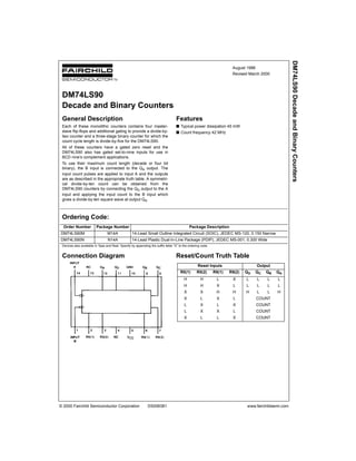
  • 1. DM74LS90 Decade and Binary Counters August 1986 Revised March 2000 DM74LS90 Decade and Binary Counters General Description Features Each of these monolithic counters contains four master- s Typical power dissipation 45 mW slave flip-flops and additional gating to provide a divide-by- s Count frequency 42 MHz two counter and a three-stage binary counter for which the count cycle length is divide-by-five for the DM74LS90. All of these counters have a gated zero reset and the DM74LS90 also has gated set-to-nine inputs for use in BCD nines complement applications. To use their maximum count length (decade or four bit binary), the B input is connected to the QA output. The input count pulses are applied to input A and the outputs are as described in the appropriate truth table. A symmetri- cal divide-by-ten count can be obtained from the DM74LS90 counters by connecting the QD output to the A input and applying the input count to the B input which gives a divide-by-ten square wave at output QA. Ordering Code: Order Number Package Number Package Description DM74LS90M M14A 14-Lead Small Outline Integrated Circuit (SOIC), JEDEC MS-120, 0.150 Narrow DM74LS90N N14A 14-Lead Plastic Dual-In-Line Package (PDIP), JEDEC MS-001, 0.300 Wide Devices also available in Tape and Reel. Specify by appending the suffix letter X to the ordering code. Connection Diagram Reset/Count Truth Table Reset Inputs Output R0(1) R0(2) R9(1) R9(2) QD QC QB QA H H L X L L L L H H X L L L L L X X H H H L L H X L X L COUNT L X L X COUNT L X X L COUNT X L L X COUNT 息 2000 Fairchild Semiconductor Corporation DS006381 www.fairchildsemi.com
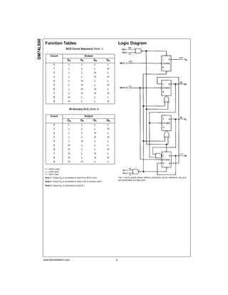
  • 2. DM74LS90 Function Tables Logic Diagram BCD Count Sequence (Note 1) Count Output QD QC QB QA 0 L L L L 1 L L L H 2 L L H L 3 L L H H 4 L H L L 5 L H L H 6 L H H L 7 L H H H 8 H L L L 9 H L L H Bi-Quinary (5-2) (Note 2) Count Output QA QD QC QB 0 L L L L 1 L L L H 2 L L H L 3 L L H H 4 L H L L 5 H L L L 6 H L L H 7 H L H L 8 H L H H 9 H H L L H = HIGH Level L = LOW Level X = Dont Care Note 1: Output QA is connected to input B for BCD count. The J and K inputs shown without connection are for reference only and are functionally at a high level. Note 2: Output QD is connected to input A for bi-quinary count. Note 3: Output QA is connected to input B. www.fairchildsemi.com 2
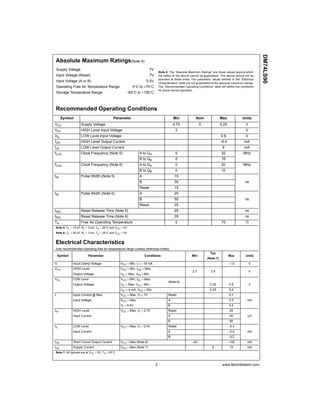
  • 3. DM74LS90 Absolute Maximum Ratings(Note 4) Supply Voltage 7V Note 4: The Absolute Maximum Ratings are those values beyond which Input Voltage (Reset) 7V the safety of the device cannot be guaranteed. The device should not be operated at these limits. The parametric values defined in the Electrical Input Voltage (A or B) 5.5V Characteristics table are not guaranteed at the absolute maximum ratings. Operating Free Air Temperature Range 0属C to +70属C The Recommended Operating Conditions table will define the conditions for actual device operation. Storage Temperature Range 65属C to +150属C Recommended Operating Conditions Symbol Parameter Min Nom Max Units VCC Supply Voltage 4.75 5 5.25 V VIH HIGH Level Input Voltage 2 V VIL LOW Level Input Voltage 0.8 V IOH HIGH Level Output Current 0.4 mA IOL LOW Level Output Current 8 mA fCLK Clock Frequency (Note 5) A to QA 0 32 MHz B to QB 0 16 fCLK Clock Frequency (Note 6) A to QA 0 20 MHz B to QB 0 10 tW Pulse Width (Note 5) A 15 B 30 ns Reset 15 tW Pulse Width (Note 6) A 25 B 50 ns Reset 25 tREL Reset Release Time (Note 5) 25 ns tREL Reset Release Time (Note 6) 35 ns TA Free Air Operating Temperature 0 70 属C Note 5: CL = 15 pF, RL = 2 k, TA = 25属C and VCC = 5V. Note 6: CL = 50 pF, RL = 2 k, TA = 25属C and VCC = 5V. Electrical Characteristics over recommended operating free air temperature range (unless otherwise noted) Typ Symbol Parameter Conditions Min Max Units (Note 7) VI Input Clamp Voltage VCC = Min, II = 18 mA 1.5 V VOH HIGH Level VCC = Min, IOH = Max 2.7 3.4 V Output Voltage VIL = Max, VIH = Min VOL LOW Level VCC = Min, IOL = Max (Note 8) Output Voltage VIL = Max, VIH = Min 0.35 0.5 V IOL = 4 mA, VCC = Min 0.25 0.4 II Input Current @ Max VCC = Max, VI = 7V Reset 0.1 Input Voltage VCC = Max A 0.2 mA VI = 5.5V B 0.4 IIH HIGH Level VCC = Max, VI = 2.7V Reset 20 Input Current A 40 袖A B 80 IIL LOW Level VCC = Max, VI = 0.4V Reset 0.4 Input Current A 2.4 mA B 3.2 IOS Short Circuit Output Current VCC = Max (Note 9) 20 100 mA ICC Supply Current VCC = Max (Note 7) 9 15 mA Note 7: All typicals are at VCC = 5V, TA = 25属C. 3 www.fairchildsemi.com
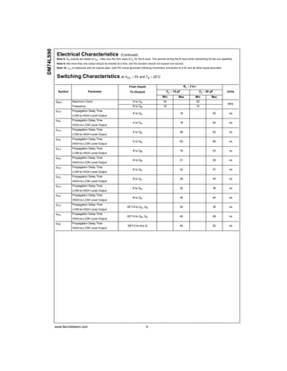
  • 4. DM74LS90 Electrical Characteristics (Continued) Note 8: QA outputs are tested at IOL = Max plus the limit value of IIL for the B input. This permits driving the B input while maintaining full fan-out capability. Note 9: Not more than one output should be shorted at a time, and the duration should not exceed one second. Note 10: ICC is measured with all outputs open, both RO inputs grounded following momentary connection to 4.5V and all other inputs grounded. Switching Characteristics at VCC = 5V and TA = 25属C From (Input) RL = 2 k Symbol Parameter To (Output) CL = 15 pF CL = 50 pF Units Min Max Min Max fMAX Maximum Clock A to QA 32 20 MHz Frequency B to QB 16 10 tPLH Propagation Delay Time A to QA 16 20 ns LOW-to-HIGH Level Output tPHL Propagation Delay Time A to QA 18 24 ns HIGH-to-LOW Level Output tPLH Propagation Delay Time A to QD 48 52 ns LOW-to-HIGH Level Output tPHL Propagation Delay Time A to QD 50 60 ns HIGH-to-LOW Level Output tPLH Propagation Delay Time B to QB 16 23 ns LOW-to-HIGH Level Output tPHL Propagation Delay Time B to QB 21 30 ns HIGH-to-LOW Level Output tPLH Propagation Delay Time B to QC 32 37 ns LOW-to-HIGH Level Output tPHL Propagation Delay Time B to QC 35 44 ns HIGH-to-LOW Level Output tPLH Propagation Delay Time B to QD 32 36 ns LOW-to-HIGH Level Output tPHL Propagation Delay Time B to QD 35 44 ns HIGH-to-LOW Level Output tPLH Propagation Delay Time SET-9 to QA, QD 30 35 ns LOW-to-HIGH Level Output tPHL Propagation Delay Time SET-9 to QB, QC 40 48 ns HIGH-to-LOW Level Output tPHL Propagation Delay Time SET-0 to Any Q 40 52 ns HIGH-to-LOW Level Output www.fairchildsemi.com 4
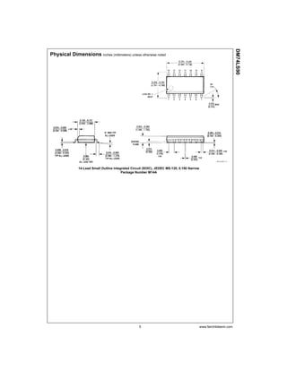
  • 5. DM74LS90 Physical Dimensions inches (millimeters) unless otherwise noted 14-Lead Small Outline Integrated Circuit (SOIC), JEDEC MS-120, 0.150 Narrow Package Number M14A 5 www.fairchildsemi.com
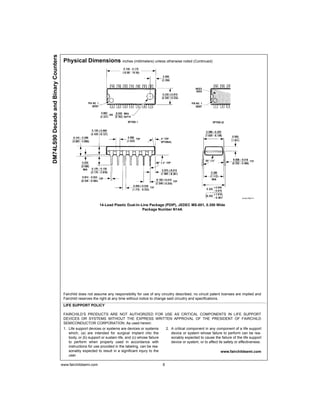
  • 6. DM74LS90 Decade and Binary Counters Physical Dimensions inches (millimeters) unless otherwise noted (Continued) 14-Lead Plastic Dual-In-Line Package (PDIP), JEDEC MS-001, 0.300 Wide Package Number N14A Fairchild does not assume any responsibility for use of any circuitry described, no circuit patent licenses are implied and Fairchild reserves the right at any time without notice to change said circuitry and specifications. LIFE SUPPORT POLICY FAIRCHILDS PRODUCTS ARE NOT AUTHORIZED FOR USE AS CRITICAL COMPONENTS IN LIFE SUPPORT DEVICES OR SYSTEMS WITHOUT THE EXPRESS WRITTEN APPROVAL OF THE PRESIDENT OF FAIRCHILD SEMICONDUCTOR CORPORATION. As used herein: 1. Life support devices or systems are devices or systems 2. A critical component in any component of a life support which, (a) are intended for surgical implant into the device or system whose failure to perform can be rea- body, or (b) support or sustain life, and (c) whose failure sonably expected to cause the failure of the life support to perform when properly used in accordance with device or system, or to affect its safety or effectiveness. instructions for use provided in the labeling, can be rea- sonably expected to result in a significant injury to the www.fairchildsemi.com user. www.fairchildsemi.com 6
  • 7. This datasheet has been downloaded from: www.DatasheetCatalog.com Datasheets for electronic components.