Pb S Nanostructures.Work At Ii Sc
1 like378 views
Lead sulfide (PbS) is a semiconductor with applications in photonics and optoelectronics. PbS nanostructures of different morphologies including flower dendrites, sheets, and rod-like structures were synthesized via hydrothermal methods. These nanostructures exhibited broad absorption spectra in the near-infrared region and photoluminescence emission around 0.6 eV. Capping the nanostructures' surfaces with organic ligands improved their optical properties by passivating surface defects. Films of PbS nanostructures embedded in a conducting polymer showed photoconductive behavior and potential for photodetector applications.
1 of 20

Recommended
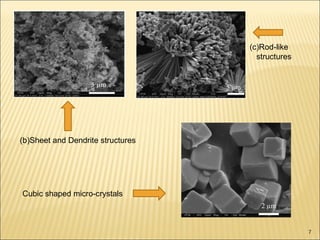
INTERNSHIP-REPORT-CHIRAS


INTERNSHIP-REPORT-CHIRASDimitris Chiras
╠²
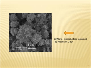
The document reports on an experiment measuring the interstitial iron concentration in multicrystalline silicon wafers using photoconductance and photoluminescence techniques. Samples underwent chemical treatment and passivation but yielded unexpectedly low minority carrier lifetimes (<20 ╬╝s) preventing analysis. Possible reasons for this include contamination during passivation from an unclean substrate holder or imperfections introduced during chemical treatment. Further experiments with a cleaned chamber could provide different results.TMS2007 Published_Marciniak_Iwanaga_Ohuchi


TMS2007 Published_Marciniak_Iwanaga_OhuchiMonika Marciniak
╠²
This document summarizes research on synthesizing and investigating the thermoelectric properties of sodium-doped vanadium pentoxide (Na-doped V2O5) thin films. A melt-quench technique was used to dope V2O5 with varying amounts of sodium. X-ray diffraction analysis showed the doped samples formed crystalline ╬▓-NaxV2O5 phase. Electrical conductivity increased by a factor of ~104 with sodium doping but the Seebeck coefficient decreased by half, resulting in an overall power factor improvement of up to ~150 times compared to pure V2O5.Determination of nonlinear absorption (╬▓) and refraction (n2)by the Z-scan me...


Determination of nonlinear absorption (╬▓) and refraction (n2)by the Z-scan me...IOSR Journals
╠²
Potassium Pentaborate nonlinear optical (NLO) material was synthesized by the solution growth method. The grown crystals were subjected to structural, optical and mechanical property studies. Crystal with excellent transparency were grown with maximum size of 9mm├Ś8mm├Ś5mm and the grown crystals were characterized by single crystal Single crystal XRD, FT-IR, TGA-DTA&DSC, and UVŌĆōvis-NIR studies. The crystal belongs to orthorhombic with a space group of mm2 having unit-cell dimensions a = 11.068├ģb= 11.175├ģ c = 9.058├ģand ╬▒ = 90┬░; ╬▓ = 90┬░; and ╬│ =90┬░; Z=4, at 298(2) K. The second-order nonlinear optical property of the polycrystalline sample has been confirmed by Kurtz-Perry powder SHG analysis. Third order nonlinear optical properties were also studied by Z-scan techniques. Nonlinear absorption and nonlinear refractive index were found out and the third order bulk susceptibility of compound was also calculated.Rotation I Presentation


Rotation I PresentationVanHoute1
╠²
The document summarizes research on the dechlorination of polychlorinated biphenyl (PCB) congeners by the anaerobic bacterium Dehalococcoides. Key findings include:
1) Dehalococcoides uses PCBs as a terminal electron acceptor and can effectively dechlorinate various PCB mixtures.
2) Experiments showed some PCB congeners (234 CB and 2345 CB) underwent more dechlorination than others (245 CB and 235 CB).
3) Further research is needed to understand congener specificity and identify reductive dehalogenase enzymes responsible for dechlorinating different PCBs.Investigation on the Growth and Physio-Chemical Properties of L-Alanine Mixed...


Investigation on the Growth and Physio-Chemical Properties of L-Alanine Mixed...IJERA Editor
╠²
Pure and L-alanine an aminoacid mixed bisthiourea cadmium bromide chloride single crystals were grown by slow evaporation technique. A drastic change in morphology was inferred with the concentration of L-alanine. Mixed crystals have better optical transparency as well as NLO efficiency than the pure BTCBC which were imperative for nonlinear applications. Also L-alanine mixing increases the hardness. The AC conductivity of the grown crystals increases with increasing concentration of L-alanine.Synthesis and Characterisation of Iron Oxide dispersed Graphene Nanocomposite.


Synthesis and Characterisation of Iron Oxide dispersed Graphene Nanocomposite.Mitul Rawat
╠²
Described process for synthesis of Iron Oxide - Graphene Nanocomposite; applications and characterization. Synthesis of nanoparticles- physical,chemical and biological


Synthesis of nanoparticles- physical,chemical and biologicalPriya Nanda
╠²
This document discusses various methods for synthesizing nanoparticles, including physical, chemical, and biological approaches. Physical methods include ball milling, melt mixing, physical vapor deposition techniques like sputtering and laser ablation. Chemical methods involve reducing metal salts or using sol-gel processes. Biological methods use microorganisms, plant extracts, proteins like ferritin, or biomolecular templates to synthesize nanoparticles. The document compares top-down lithography approaches to bottom-up assembly and provides many examples of synthesizing specific nanomaterials.sci comm research-vivek


sci comm research-vivekVivek Saraswat
╠²
This document discusses nanoporous graphene (NPG) fabrication methods, ion and gas permeation mechanisms through NPG, and presents preliminary experimental results. It summarizes that NPG has potential for desalination and gas separation due to high permeability from atomic thickness and strength to withstand high pressures. Permeation is dependent on pore size and functionalization, which can be used to control selectivity. The author's project aims to experimentally investigate ion selectivity of graphene nanopores and verify computational results by measuring ionic conductivity across graphene membranes using a setup that seals nanopores with graphene. Representative results show graphene seals 150nm pores and ion-voltage curves with and without sealed pores.The Effect of Size of the CuO Nanoleaves on the Sunlight Driven Photocatalyti...


The Effect of Size of the CuO Nanoleaves on the Sunlight Driven Photocatalyti...IRJET Journal
╠²
This document summarizes research on the effect of surfactant concentration on the size and photocatalytic properties of copper oxide nano leaves. Copper oxide nano leaves were synthesized using different concentrations of polyvinyl pyrrolidone (PVP) as a surfactant. Characterization with XRD, FTIR and SEM showed that increasing PVP concentration decreased particle size and altered morphology from narrow leaves to shortened, broadened leaves. Photocatalytic testing demonstrated that the sample with the highest PVP concentration degraded Congo Red dye in sunlight most effectively within 4 hours, indicating smaller size and higher surface area enhanced photocatalytic activity.Onyeachu et al., 2014


Onyeachu et al., 2014Ikenna Onyeachu
╠²
1) The study examines the corrosion behavior of electrodeposited Ni-Al composite coating containing 1╬╝m aluminum particles in 3.5% NaCl + 0.05 M H2SO4 solution.
2) Open circuit potential measurements showed the aluminum particles shifted the Ni corrosion potential to more negative values. Potentiodynamic polarization tests revealed the aluminum particles increased the corrosion rate of the Ni coating by enhancing both the cathodic and anodic reactions.
3) XPS characterization confirmed the aluminum corrosion products were highly soluble in the test solution. This disturbed the formation of a continuous protective nickel corrosion product layer, as shown by SEM analysis.synthesis of fly ash based zeolite for wastewater purification


synthesis of fly ash based zeolite for wastewater purificationVinit Sehgal
╠²
This document summarizes the development of a novel zeolite synthesized from fly ash for treating wastewater. The synthesis process involves mixing fly ash with sodium hydroxide and refluxing for 98 hours at 383K until neutral pH is reached. This combination of conventional and microwave synthesis increases the zeolite's porosity and cation exchange capacity (CEC) for effective wastewater treatment. Characterization tests and efficiency tests were performed to evaluate the zeolite's ability to remove various cations and anions from wastewater via ion exchange and adsorption. Process optimization studies examined factors like CEC, pH control, reaction time and temperature to improve the zeolite synthesis.Coupling_Carrots


Coupling_CarrotsScott Shaw
╠²
Scott Shaw conducted research investigating strong coupling of ╬▓-carotene in microcavities. He was successful in achieving the strong coupling regime, obtaining a Rabi splitting of ~2.1 eV, over twice as large as the next highest. Degradation experiments showed ╬▓-carotene films deteriorated quickly when exposed to light and water, but less so under nitrogen. While a large splitting was achieved, the system was likely not emissive due to aggregation-induced quenching. The research demonstrated strong coupling of ╬▓-carotene can be achieved under specified fabrication and storage conditions.Synthesis and Characterization of Silica-Nickel Nanocomposite through sol-gel...


Synthesis and Characterization of Silica-Nickel Nanocomposite through sol-gel...IJRES Journal
╠²
The optimum combination of experimental variables- temperature, time of heat treatment under nitrogen atmosphere and amount of Ni-salt was delineated to find the maximum yield of nanophase Ni in the silica gel matrix. The size of Ni in the silica gel was found in the range 35 and 61nm. In the last two decades synthesis, characterization and understanding a material with lower dimensions have become the most interesting area of research due to their novel properties and potential applications in different fields. : CuTiB2


CuTiB2Rannesh Lokesh
╠²
This document summarizes a study on the irradiation-induced nanostructuring of Cu-TiB2 thin films with krypton ions. Room temperature irradiation led to the precipitation of ~4 nm cubic TiB nanoparticles, while irradiation at 650┬░C resulted in ~5 nm hexagonal TiB2 precipitates. The precipitate size and density (~2-3 ├Ś 1023 m-3) remained unchanged with increased dose from 1 ├Ś 1016 to 3 ├Ś 1016 ions/cm2 at 650┬░C, indicating a stable nanostructure formed. No extended defects were detected even at the highest dose, suggesting this nanostructuring imparts high radiation resistance.seminar presentation


seminar presentationTeh Joo Foon
╠²
The document summarizes the total synthesis of (┬▒)-spiroindimicins B and C, which are alkaloids isolated from a deep-sea marine actinomycete. Key steps in the synthesis include installing a spirocenter using an intramolecular Heck reaction, forming a pentacyclic spirobisindole through Fischer indolization, and constructing a trisubstituted pyrrole ring via a late-stage Sch├ČllkopfŌĆōMagnusŌĆōBartonŌĆōZard reaction. The synthesis confirms the unique heteroaromatic structure of these natural products and demonstrates the use of mild reactions to install functional groups like the spirocenter and pyrrole ring.Honors -Chemistry 1011


Honors -Chemistry 1011Michael Edgar
╠²
The document discusses various topics related to biological chemistry including water and its properties, plant transport of water, solubility of substances in water, and the carbon cycle. It includes figures and diagrams related to these topics as well as questions about emergent properties in red harvester ants, the bicarbonate buffer system, and the global carbon cycle.TCE Plume Remediation via ISCR-Enhanced Bioremediation


TCE Plume Remediation via ISCR-Enhanced BioremediationWeirdTurnPro
╠²
Updated results of field pilot of integrated use of EHC+KB-1 for TCE Remediation. Originally published in Fall 2008 issue of Remediation.Doping of graphene and its application in photo electrochemical water splitting


Doping of graphene and its application in photo electrochemical water splittingDr. Basudev Baral
╠²
Doping of graphene with heteroatoms like nitrogen and boron can effectively tune its electronic structure and properties. This makes doped graphene suitable for applications like photocatalytic water splitting. Nitrogen or boron doping creates a bandgap, allowing graphene to be used as a photocatalyst under visible light. Composites of nitrogen-doped graphene and other semiconductors like CdS have shown higher hydrogen evolution rates from water under visible light compared to the semiconductors alone. Perfectly designed, doped graphene with the proper bandgap could enable water splitting using only visible light from the sun.Publication 1 (2013)


Publication 1 (2013)Natalia Pawlowska
╠²
The document summarizes a study that used a scanning Kelvin probe to characterize the surface modification of indium tin oxide (ITO) substrates with photopatternable silane adlayers. A photoreactive silane molecule containing an o-nitrobenzyl group was used to form self-assembled monolayers on ITO. UV light through a photomask was used to selectively remove regions of the silane layer, and changes in surface potential were detected using contact potential difference measurements from the scanning Kelvin probe. Additional characterization techniques including X-ray photoelectron spectroscopy and contact angle measurements were also used to analyze the modified surfaces.Growth, characterization, and antibacterial studies of L-Lysine single crysta...


Growth, characterization, and antibacterial studies of L-Lysine single crysta...IOSRJAP
╠²
Single crystals of L-lysine added Potassium Bromide were grown by slow evaporation technique at room temperature. The crystalline nature of the grown crystal wasconfirmed using powder X-ray diffraction technique. Single crystal X-ray diffraction patterns were recorded for the structural conformation and it was found to be cubic. The UV ŌĆōVIS- NIR Spectrum of the grown crystals shows less optical absorption and good transmittance in the entire visible region enabling its use in optical applications. Vickers micro hardness test was carried out to analyze the mechanical property of the grown L- lysine potassium Bromide single crystal. Thermo gravimetric analysis proved that the crystal is stable up to 600┬║C. The frequency and temperature dependence of dielectric constant (╬Ąr), dielectric loss (tan ╬┤) were also measured. The grown crystal was evaluated for its biological efficacy and found to exhibit anti bacterial activities against some select bacterial strains.Semianr Presentation


Semianr PresentationMohamed Hamda, EIT, MASc, FE
╠²
1) The presentation discusses the effect of initial surface condition on pool boiling of nanofluids. Recent research has found that nanofluid heat transfer performance is greatly affected by nanoparticles depositing on the heated surface during boiling.
2) The current research uses new precision machining techniques to create consistent surface textures and surfactants to enhance nanofluid stability and prevent nanoparticle deposition. Experimental results show that surfactant addition eliminates deposition and improves heat transfer.
3) Heat transfer is also influenced by surface roughness, with rougher surfaces enhancing boiling. However, when nanoparticle size is larger than surface roughness features, deposition does not occur and heat transfer is improved with or without surfactant addition. The research aimsCoimbra 2008 2


Coimbra 2008 2Pedro Vidinha
╠²
The document describes Ion Jelly, a new conducting and biocompatible material made by mixing gelatin with ionic liquids. Ion Jelly is light, flexible, thermally stable up to 180┬░C, and has conductivity above 10-4 S/cm. It can be adjusted to various surfaces and is environmentally friendly. Ion Jelly shows potential for applications such as biosensors and electron transfer due to its ability to immobilize proteins while maintaining their activity.Final IBB_poster


Final IBB_posterDaniel Solis
╠²
The document summarizes research on using bovine serum albumin (BSA) and glutaraldehyde to preserve the structure of gold nanoparticle aggregates formed through controlled salt-induced aggregation. Specifically:
- NaCl is used to induce aggregation of citrate-stabilized gold nanoparticles observed through red-shifting of UV-Vis spectra.
- Addition of BSA halts aggregation and stabilizes aggregate structures by coating nanoparticles and clusters with a protein corona.
- Glutaraldehyde crosslinks the BSA, preserving aggregate morphology which is observed using dark-field microscopy and SEM.
- The technique allows exploration of plasmon coupling in controlled nanoparticle assemblies through optical spectroscopy of stabilized structures.Research Summary Document October 28 2015


Research Summary Document October 28 2015Kevin Yuan
╠²
This document provides a summary of several papers that studied various surface species and gases generated by different plasma sources, including microplasmas, dielectric barrier discharges (DBDs), atmospheric pressure plasma jets (APPJs), and corona discharges. The sources operated in various gas mixtures including water vapor, air, argon, nitrogen, oxygen and analyzed surface species like OH, NO, O using spectroscopy. The papers investigated applications such as biomass and polymer surface treatment, sterilization, tissue ablation and semiconductor processing. ppt on characterization and synthesis of nanofluid with base fluid water


ppt on characterization and synthesis of nanofluid with base fluid waterabhishek singh
╠²
This document summarizes the synthesis and characterization of a nanofluid with water as the base fluid. It discusses the types of nanoparticles and nanofluids, describes the synthesis of cerium oxide nanoparticles and the nanofluid, and presents the experimental methodology used to measure properties like density, viscosity, and thermal conductivity of the nanofluid at varying temperatures and nanoparticle concentrations. The results show that the density, viscosity, and thermal conductivity of the nanofluid increase with increasing nanoparticle concentration. The maximum thermal conductivity achieved is 0.747 W/m-K at a concentration of 1.5% and temperature of 75┬░C.ELECTRODEPOSITION OF SILVER NANOPARTICLES ON CARBON SPHERE SURFACES BY PULSE ...


ELECTRODEPOSITION OF SILVER NANOPARTICLES ON CARBON SPHERE SURFACES BY PULSE ...International Journal of Technical Research & Application
╠²
This document summarizes research on electrodepositing silver nanoparticles onto carbon sphere surfaces using a pulse current. Key findings include:
1) Silver nanoparticles were successfully electrodeposited with a size of 100-400nm after 2 minutes using a pulse current.
2) Deposition occurred on accessible carbon surface sites, forming a monolayer of scattered nanoparticles. Continued deposition led to larger particles and multilayers.
3) Pulse current helped manage monolayer deposition compared to direct current, controlling particle size and number of layers.Photocatalytic Properties of GO-(Cd0.8-Zn0.2)S Nanocomposites Prepared by Che...


Photocatalytic Properties of GO-(Cd0.8-Zn0.2)S Nanocomposites Prepared by Che...IJLT EMAS
╠²
Graphene oxide - (Cd0.8-Zn0.2)S nanocomposite
material was synthesized by the simple and economically viable
chemical precipitation method at different temperatures and its
photocatalytic properties were investigated. Measurement of
photocatalytic degradation of Rhodamine B dye was carried out
under visible light. The photocatalytic efficiency of the
synthesized nanocomposites was calculated and the effect of bath
temperature on the photocatalytic efficiency was studied. The
studies suggest that the prepared nanocomposites exhibit
reasonably good photocatalytic properties. Better photocatalysis
is observed at lower bath temperatures for preparation of the
nanocomposites. Photocatalytic efficiency close to 70% has been
obtained for the synthesised GO-(Cd0.8-Zn0.2) S nanocomposites
which can be further improved by optimizing the preparative
conditionsSynthesis and characterization of pure zinc oxide nanoparticles and nickel do...


Synthesis and characterization of pure zinc oxide nanoparticles and nickel do...eSAT Journals
╠²
Abstract In this paper, Zinc oxide nanoparticles are synthesized by simple wet chemical precipitation method. Zinc nitrate and sodium hydroxide are used as the starting materials.Zinc oxide nanoparticles are formed at a very low temperature of the order of 800C. Nickel doped zinc oxide nanoparticles are synthesized in two steps. In first step precipitate is obtained by reduction of mixture of zinc nitrate, ferric nitrate and starch by sodium hydroxide solution while in second step the given precipitate is thermally decomposed at high temperature of the order of 4000C. The crystallinity of the synthesized nanoparticles is then confirmed by X ray diffraction spectroscopy (XRD).The elemental composition of the powder is detected by Energy Dispersive X ray spectroscopy (EDAX). The morphology of the powder is investigated by Scanning Electron Microscopy (SEM). Magnetic characterization of nickel doped zinc oxide nanoparticles is done by Squid Magnetometer. Low temperature magnetization behavior revealed ferromagnetic behavior of sample. Key Words: Zinc oxide nanoparticles, Nickel doped ZnO, Antibacterial activity, Squid magnetometer, SEMfinal draft of paper


final draft of paperWesley Hock
╠²
- The document studies using water as an alternative solvent to the commonly used acetonitrile for applying organic layers from diazonium salts.
- When using water, the diazonium salt solution had to be replaced every couple days to maintain a consistent concentration, as the salt decomposed over time, turning the solution orange.
- Preliminary results found that layers could be applied using water as a solvent, but it may lack control over completeness of the layer compared to acetonitrile.H0354854


H0354854IOSR Journals
╠²
IOSR Journal of Applied Chemistry (IOSR-JAC) is an open access international journal that provides rapid publication (within a month) of articles in all areas of applied chemistry and its applications. The journal welcomes publications of high quality papers on theoretical developments and practical applications in Chemical Science. Original research papers, state-of-the-art reviews, and high quality technical notes are invited for publications.More Related Content
What's hot (20)
The Effect of Size of the CuO Nanoleaves on the Sunlight Driven Photocatalyti...


The Effect of Size of the CuO Nanoleaves on the Sunlight Driven Photocatalyti...IRJET Journal
╠²
This document summarizes research on the effect of surfactant concentration on the size and photocatalytic properties of copper oxide nano leaves. Copper oxide nano leaves were synthesized using different concentrations of polyvinyl pyrrolidone (PVP) as a surfactant. Characterization with XRD, FTIR and SEM showed that increasing PVP concentration decreased particle size and altered morphology from narrow leaves to shortened, broadened leaves. Photocatalytic testing demonstrated that the sample with the highest PVP concentration degraded Congo Red dye in sunlight most effectively within 4 hours, indicating smaller size and higher surface area enhanced photocatalytic activity.Onyeachu et al., 2014


Onyeachu et al., 2014Ikenna Onyeachu
╠²
1) The study examines the corrosion behavior of electrodeposited Ni-Al composite coating containing 1╬╝m aluminum particles in 3.5% NaCl + 0.05 M H2SO4 solution.
2) Open circuit potential measurements showed the aluminum particles shifted the Ni corrosion potential to more negative values. Potentiodynamic polarization tests revealed the aluminum particles increased the corrosion rate of the Ni coating by enhancing both the cathodic and anodic reactions.
3) XPS characterization confirmed the aluminum corrosion products were highly soluble in the test solution. This disturbed the formation of a continuous protective nickel corrosion product layer, as shown by SEM analysis.synthesis of fly ash based zeolite for wastewater purification


synthesis of fly ash based zeolite for wastewater purificationVinit Sehgal
╠²
This document summarizes the development of a novel zeolite synthesized from fly ash for treating wastewater. The synthesis process involves mixing fly ash with sodium hydroxide and refluxing for 98 hours at 383K until neutral pH is reached. This combination of conventional and microwave synthesis increases the zeolite's porosity and cation exchange capacity (CEC) for effective wastewater treatment. Characterization tests and efficiency tests were performed to evaluate the zeolite's ability to remove various cations and anions from wastewater via ion exchange and adsorption. Process optimization studies examined factors like CEC, pH control, reaction time and temperature to improve the zeolite synthesis.Coupling_Carrots


Coupling_CarrotsScott Shaw
╠²
Scott Shaw conducted research investigating strong coupling of ╬▓-carotene in microcavities. He was successful in achieving the strong coupling regime, obtaining a Rabi splitting of ~2.1 eV, over twice as large as the next highest. Degradation experiments showed ╬▓-carotene films deteriorated quickly when exposed to light and water, but less so under nitrogen. While a large splitting was achieved, the system was likely not emissive due to aggregation-induced quenching. The research demonstrated strong coupling of ╬▓-carotene can be achieved under specified fabrication and storage conditions.Synthesis and Characterization of Silica-Nickel Nanocomposite through sol-gel...


Synthesis and Characterization of Silica-Nickel Nanocomposite through sol-gel...IJRES Journal
╠²
The optimum combination of experimental variables- temperature, time of heat treatment under nitrogen atmosphere and amount of Ni-salt was delineated to find the maximum yield of nanophase Ni in the silica gel matrix. The size of Ni in the silica gel was found in the range 35 and 61nm. In the last two decades synthesis, characterization and understanding a material with lower dimensions have become the most interesting area of research due to their novel properties and potential applications in different fields. : CuTiB2


CuTiB2Rannesh Lokesh
╠²
This document summarizes a study on the irradiation-induced nanostructuring of Cu-TiB2 thin films with krypton ions. Room temperature irradiation led to the precipitation of ~4 nm cubic TiB nanoparticles, while irradiation at 650┬░C resulted in ~5 nm hexagonal TiB2 precipitates. The precipitate size and density (~2-3 ├Ś 1023 m-3) remained unchanged with increased dose from 1 ├Ś 1016 to 3 ├Ś 1016 ions/cm2 at 650┬░C, indicating a stable nanostructure formed. No extended defects were detected even at the highest dose, suggesting this nanostructuring imparts high radiation resistance.seminar presentation


seminar presentationTeh Joo Foon
╠²
The document summarizes the total synthesis of (┬▒)-spiroindimicins B and C, which are alkaloids isolated from a deep-sea marine actinomycete. Key steps in the synthesis include installing a spirocenter using an intramolecular Heck reaction, forming a pentacyclic spirobisindole through Fischer indolization, and constructing a trisubstituted pyrrole ring via a late-stage Sch├ČllkopfŌĆōMagnusŌĆōBartonŌĆōZard reaction. The synthesis confirms the unique heteroaromatic structure of these natural products and demonstrates the use of mild reactions to install functional groups like the spirocenter and pyrrole ring.Honors -Chemistry 1011


Honors -Chemistry 1011Michael Edgar
╠²
The document discusses various topics related to biological chemistry including water and its properties, plant transport of water, solubility of substances in water, and the carbon cycle. It includes figures and diagrams related to these topics as well as questions about emergent properties in red harvester ants, the bicarbonate buffer system, and the global carbon cycle.TCE Plume Remediation via ISCR-Enhanced Bioremediation


TCE Plume Remediation via ISCR-Enhanced BioremediationWeirdTurnPro
╠²
Updated results of field pilot of integrated use of EHC+KB-1 for TCE Remediation. Originally published in Fall 2008 issue of Remediation.Doping of graphene and its application in photo electrochemical water splitting


Doping of graphene and its application in photo electrochemical water splittingDr. Basudev Baral
╠²
Doping of graphene with heteroatoms like nitrogen and boron can effectively tune its electronic structure and properties. This makes doped graphene suitable for applications like photocatalytic water splitting. Nitrogen or boron doping creates a bandgap, allowing graphene to be used as a photocatalyst under visible light. Composites of nitrogen-doped graphene and other semiconductors like CdS have shown higher hydrogen evolution rates from water under visible light compared to the semiconductors alone. Perfectly designed, doped graphene with the proper bandgap could enable water splitting using only visible light from the sun.Publication 1 (2013)


Publication 1 (2013)Natalia Pawlowska
╠²
The document summarizes a study that used a scanning Kelvin probe to characterize the surface modification of indium tin oxide (ITO) substrates with photopatternable silane adlayers. A photoreactive silane molecule containing an o-nitrobenzyl group was used to form self-assembled monolayers on ITO. UV light through a photomask was used to selectively remove regions of the silane layer, and changes in surface potential were detected using contact potential difference measurements from the scanning Kelvin probe. Additional characterization techniques including X-ray photoelectron spectroscopy and contact angle measurements were also used to analyze the modified surfaces.Growth, characterization, and antibacterial studies of L-Lysine single crysta...


Growth, characterization, and antibacterial studies of L-Lysine single crysta...IOSRJAP
╠²
Single crystals of L-lysine added Potassium Bromide were grown by slow evaporation technique at room temperature. The crystalline nature of the grown crystal wasconfirmed using powder X-ray diffraction technique. Single crystal X-ray diffraction patterns were recorded for the structural conformation and it was found to be cubic. The UV ŌĆōVIS- NIR Spectrum of the grown crystals shows less optical absorption and good transmittance in the entire visible region enabling its use in optical applications. Vickers micro hardness test was carried out to analyze the mechanical property of the grown L- lysine potassium Bromide single crystal. Thermo gravimetric analysis proved that the crystal is stable up to 600┬║C. The frequency and temperature dependence of dielectric constant (╬Ąr), dielectric loss (tan ╬┤) were also measured. The grown crystal was evaluated for its biological efficacy and found to exhibit anti bacterial activities against some select bacterial strains.Semianr Presentation


Semianr PresentationMohamed Hamda, EIT, MASc, FE
╠²
1) The presentation discusses the effect of initial surface condition on pool boiling of nanofluids. Recent research has found that nanofluid heat transfer performance is greatly affected by nanoparticles depositing on the heated surface during boiling.
2) The current research uses new precision machining techniques to create consistent surface textures and surfactants to enhance nanofluid stability and prevent nanoparticle deposition. Experimental results show that surfactant addition eliminates deposition and improves heat transfer.
3) Heat transfer is also influenced by surface roughness, with rougher surfaces enhancing boiling. However, when nanoparticle size is larger than surface roughness features, deposition does not occur and heat transfer is improved with or without surfactant addition. The research aimsCoimbra 2008 2


Coimbra 2008 2Pedro Vidinha
╠²
The document describes Ion Jelly, a new conducting and biocompatible material made by mixing gelatin with ionic liquids. Ion Jelly is light, flexible, thermally stable up to 180┬░C, and has conductivity above 10-4 S/cm. It can be adjusted to various surfaces and is environmentally friendly. Ion Jelly shows potential for applications such as biosensors and electron transfer due to its ability to immobilize proteins while maintaining their activity.Final IBB_poster


Final IBB_posterDaniel Solis
╠²
The document summarizes research on using bovine serum albumin (BSA) and glutaraldehyde to preserve the structure of gold nanoparticle aggregates formed through controlled salt-induced aggregation. Specifically:
- NaCl is used to induce aggregation of citrate-stabilized gold nanoparticles observed through red-shifting of UV-Vis spectra.
- Addition of BSA halts aggregation and stabilizes aggregate structures by coating nanoparticles and clusters with a protein corona.
- Glutaraldehyde crosslinks the BSA, preserving aggregate morphology which is observed using dark-field microscopy and SEM.
- The technique allows exploration of plasmon coupling in controlled nanoparticle assemblies through optical spectroscopy of stabilized structures.Research Summary Document October 28 2015


Research Summary Document October 28 2015Kevin Yuan
╠²
This document provides a summary of several papers that studied various surface species and gases generated by different plasma sources, including microplasmas, dielectric barrier discharges (DBDs), atmospheric pressure plasma jets (APPJs), and corona discharges. The sources operated in various gas mixtures including water vapor, air, argon, nitrogen, oxygen and analyzed surface species like OH, NO, O using spectroscopy. The papers investigated applications such as biomass and polymer surface treatment, sterilization, tissue ablation and semiconductor processing. ppt on characterization and synthesis of nanofluid with base fluid water


ppt on characterization and synthesis of nanofluid with base fluid waterabhishek singh
╠²
This document summarizes the synthesis and characterization of a nanofluid with water as the base fluid. It discusses the types of nanoparticles and nanofluids, describes the synthesis of cerium oxide nanoparticles and the nanofluid, and presents the experimental methodology used to measure properties like density, viscosity, and thermal conductivity of the nanofluid at varying temperatures and nanoparticle concentrations. The results show that the density, viscosity, and thermal conductivity of the nanofluid increase with increasing nanoparticle concentration. The maximum thermal conductivity achieved is 0.747 W/m-K at a concentration of 1.5% and temperature of 75┬░C.ELECTRODEPOSITION OF SILVER NANOPARTICLES ON CARBON SPHERE SURFACES BY PULSE ...


ELECTRODEPOSITION OF SILVER NANOPARTICLES ON CARBON SPHERE SURFACES BY PULSE ...International Journal of Technical Research & Application
╠²
This document summarizes research on electrodepositing silver nanoparticles onto carbon sphere surfaces using a pulse current. Key findings include:
1) Silver nanoparticles were successfully electrodeposited with a size of 100-400nm after 2 minutes using a pulse current.
2) Deposition occurred on accessible carbon surface sites, forming a monolayer of scattered nanoparticles. Continued deposition led to larger particles and multilayers.
3) Pulse current helped manage monolayer deposition compared to direct current, controlling particle size and number of layers.Photocatalytic Properties of GO-(Cd0.8-Zn0.2)S Nanocomposites Prepared by Che...


Photocatalytic Properties of GO-(Cd0.8-Zn0.2)S Nanocomposites Prepared by Che...IJLT EMAS
╠²
Graphene oxide - (Cd0.8-Zn0.2)S nanocomposite
material was synthesized by the simple and economically viable
chemical precipitation method at different temperatures and its
photocatalytic properties were investigated. Measurement of
photocatalytic degradation of Rhodamine B dye was carried out
under visible light. The photocatalytic efficiency of the
synthesized nanocomposites was calculated and the effect of bath
temperature on the photocatalytic efficiency was studied. The
studies suggest that the prepared nanocomposites exhibit
reasonably good photocatalytic properties. Better photocatalysis
is observed at lower bath temperatures for preparation of the
nanocomposites. Photocatalytic efficiency close to 70% has been
obtained for the synthesised GO-(Cd0.8-Zn0.2) S nanocomposites
which can be further improved by optimizing the preparative
conditionsSynthesis and characterization of pure zinc oxide nanoparticles and nickel do...


Synthesis and characterization of pure zinc oxide nanoparticles and nickel do...eSAT Journals
╠²
Abstract In this paper, Zinc oxide nanoparticles are synthesized by simple wet chemical precipitation method. Zinc nitrate and sodium hydroxide are used as the starting materials.Zinc oxide nanoparticles are formed at a very low temperature of the order of 800C. Nickel doped zinc oxide nanoparticles are synthesized in two steps. In first step precipitate is obtained by reduction of mixture of zinc nitrate, ferric nitrate and starch by sodium hydroxide solution while in second step the given precipitate is thermally decomposed at high temperature of the order of 4000C. The crystallinity of the synthesized nanoparticles is then confirmed by X ray diffraction spectroscopy (XRD).The elemental composition of the powder is detected by Energy Dispersive X ray spectroscopy (EDAX). The morphology of the powder is investigated by Scanning Electron Microscopy (SEM). Magnetic characterization of nickel doped zinc oxide nanoparticles is done by Squid Magnetometer. Low temperature magnetization behavior revealed ferromagnetic behavior of sample. Key Words: Zinc oxide nanoparticles, Nickel doped ZnO, Antibacterial activity, Squid magnetometer, SEMELECTRODEPOSITION OF SILVER NANOPARTICLES ON CARBON SPHERE SURFACES BY PULSE ...


ELECTRODEPOSITION OF SILVER NANOPARTICLES ON CARBON SPHERE SURFACES BY PULSE ...International Journal of Technical Research & Application
╠²
Similar to Pb S Nanostructures.Work At Ii Sc (20)
final draft of paper


final draft of paperWesley Hock
╠²
- The document studies using water as an alternative solvent to the commonly used acetonitrile for applying organic layers from diazonium salts.
- When using water, the diazonium salt solution had to be replaced every couple days to maintain a consistent concentration, as the salt decomposed over time, turning the solution orange.
- Preliminary results found that layers could be applied using water as a solvent, but it may lack control over completeness of the layer compared to acetonitrile.H0354854


H0354854IOSR Journals
╠²
IOSR Journal of Applied Chemistry (IOSR-JAC) is an open access international journal that provides rapid publication (within a month) of articles in all areas of applied chemistry and its applications. The journal welcomes publications of high quality papers on theoretical developments and practical applications in Chemical Science. Original research papers, state-of-the-art reviews, and high quality technical notes are invited for publications.Electrodeposited Ru Nanoparticles for Electrochemical Reduction of NAD+ to NADH


Electrodeposited Ru Nanoparticles for Electrochemical Reduction of NAD+ to NADHNorth Breeze
╠²
This document summarizes research on the electrodeposition of ruthenium nanoparticles on glassy carbon substrates for electrocatalytic reduction of NAD+. Scanning electron microscopy showed that deposition potential influences nanoparticle size and density, with more negative potentials producing smaller, more densely packed nanoparticles. Electrodes with higher nanoparticle density showed lower overpotentials for hydrogen evolution and catalytic activity for NAD+ reduction. The most negative deposition potential produced a ruthenium film with distinct electrochemical behavior, showing high activity for hydrogen evolution. Overall, controlling deposition potential allows tuning of ruthenium nanoparticle morphology for electrocatalytic applications.BUIE21 Jan 15


BUIE21 Jan 15Alokmay Datta
╠²
This document summarizes research on using self-organization phenomena like dewetting and demixing to form nanocrystals. Dewetting of thin films can cause the formation of nanodroplets. Demixing in liquid crystals provides an ordered matrix for nanoparticle growth. Specifically, zinc stearate nanocrystals were formed by dewetting on cadmium and cobalt stearate templates. The nanocrystals had different structures depending on the template. Also, gold nano-prisms were formed in the liquid crystal MBBA using its functional groups to reduce gold salt and provide ordering during demixing. Characterization showed the highly crystalline nature of the nanoparticles.New Material:Perovskites presentation


New Material:Perovskites presentationJohn Shiloba Pishikeni
╠²
Perovskite is a new material with great potentials to solving problems of electrical and power engineering.SnO2 Nanospheres J All Comp


SnO2 Nanospheres J All Compazhar fakharuddin
╠²
1) Tin oxide nanostructures were synthesized via a hydrothermal process to optimize their morphology for use as photoanodes in dye-sensitized solar cells.
2) Samples synthesized at different temperatures resulted in different nanostructure morphologies. The sample synthesized at 200┬░C showed an optimal mixture of tin oxide nanoparticles and hollow nanospheres.
3) When used as a photoanode, the optimized tin oxide nanostructures synthesized at 200┬░C achieved the highest photovoltaic conversion efficiency of 7.5%, the highest reported for pristine tin oxide at the time.Cu doped to zno


Cu doped to znoalisanim2
╠²
The document discusses copper-doped ZnO nanoparticles prepared by precipitation method with varying copper contents. Characterization techniques including XRD, XPS, EPR, TG-DTA and BET were used. XRD showed the crystallite sizes were 45-49 nm. XPS showed copper ions exist as isolated Cu2+ on the particle surfaces. EPR confirmed isolated Cu2+ ions. Photocatalytic testing showed degradation of Reactive Black 5 dye under UV light. Pure ZnO showed the best photocatalytic activity among the samples.NANOMATERIAL


NANOMATERIALArchanaKR11
╠²
This document summarizes the synthesis, characterization, and photocatalytic study of neodymium-doped cerium oxide nanoparticles. Cerium oxide and cerium oxide doped with neodymium in different ratios were synthesized via a sol-gel method and characterized using XRD, FT-IR, and TGA/DSC. XRD and FT-IR analysis confirmed the formation of cerium oxide with a cubic fluorite structure without phase changes after calcination. TGA/DSC showed the thermal stability of the samples. Photocatalytic testing found that doping with neodymium, especially at a ratio of 100:10, improved the photocatalytic activity for degrading methylene blue dyePerovskite solar cells - An Introduction, By Dawn John Mullassery


Perovskite solar cells - An Introduction, By Dawn John MullasseryDawn John Mullassery
╠²
Perovskite solar cells (PSCs) are a promising photovoltaic technology that has seen rapid increases in power conversion efficiency from 9.7% to over 20% in just a few years. PSCs offer advantages over other solar cell technologies in terms of cost of raw materials, fabrication, and efficiency. However, research is still needed to address challenges such as stability in the presence of moisture and the toxicity of lead used in early PSC designs. Future work aims to remove toxicity concerns and develop thin film and flexible PSC designs to enable widespread commercialization of this emerging solar technology.Perovskite Crystals: A Bright Future in Solar Technology


Perovskite Crystals: A Bright Future in Solar TechnologyReid Barton
╠²
1) The student created perovskite crystal solar cells using different precursor solutions and measured their voltage outputs. Cells using a 2:1 ratio of formamidinium chloride to lead iodide performed best, achieving up to 520 mV.
2) A tandem cell combining perovskite and silicon layers performed better than either individually, demonstrating potential for improved efficiencies.
3) The higher chloride concentration in the optimal precursor solution likely increased the crystal's band gap, resulting in a higher output voltage. While rudimentary, the experiments provided insight into effective precursor compositions.Role of adsorbing moieties on thermal conductivity and associated properties ...


Role of adsorbing moieties on thermal conductivity and associated properties ...Regina Duque
╠²
This document summarizes a study on the role of adsorbing moieties (surface active species) on the thermal conductivity and other properties of nanofluids. The study examines how surface active species affect thermal conductivity, rheology, density, contact angle, and refractive index. It also investigates how the initial thermal conductivity, morphology, and number density of particles influence thermal conductivity enhancement in nanofluids. The results show that adsorbed surface active species can enhance nanofluid stability without lowering thermal conductivity enhancement. Thermal conductivity was found to follow effective medium theory for both "soft" and "hard" sphere particles. Particle orientation and aspect ratio were also found to impact thermal conductivity.Glen Junor Senior Thesis


Glen Junor Senior ThesisGlen Junor
╠²
The document summarizes research on the stability of lead telluride (PbTe) quantum dots. PbTe QDs show promising properties for optoelectronic devices but are unstable when exposed to oxygen. The document studies the oxidation of various sized PbTe and lead selenide (PbSe) QDs over time when exposed to air and nitrogen. PbTe QDs oxidize much more rapidly than PbSe QDs when in solution. However, coating PbTe QD films with alumina provides effective long-term protection from oxidation.Characterisation of NanostructuredLead Selenide (PbSe) Thin Films for Solar D...


Characterisation of NanostructuredLead Selenide (PbSe) Thin Films for Solar D...IOSR Journals
╠²
The document summarizes research characterizing nanostructured lead selenide (PbSe) thin films deposited using chemical bath deposition for potential solar device applications. PbSe thin films were deposited on glass substrates at varying pH levels of the deposition bath. Characterization of the structural, optical and electrical properties of the films showed that film thickness and properties like band gap energy and conductivity could be controlled by varying the deposition parameters like pH. Higher pH levels resulted in films with lower conductivity and band gap, indicating the properties of PbSe could be tuned for different functions. The nanostructured PbSe thin films showed potential for use in solar energy devices based on their optical absorption properties.Nitrogen-Enriched Carbon Nanobubbles and Nanospheres for Applications in Ener...


Nitrogen-Enriched Carbon Nanobubbles and Nanospheres for Applications in Ener...Devika Laishram
╠²
Multifunctional carbon nanomaterials have attracted remarkable consideration for use in various energy
conversion and storage devices because of their ultrahigh specific
surface area, unique morphology, and excellent electrochemical
properties. Herein, we report the synthesis of highly uniform and
ordered nitrogen-enriched carbon nanospheres (CS) and nanobubbles (CNB) by a modified Sto╠łber reaction using resorcinol and
formaldehyde in the presence of ethylenediamine as a nitrogen
source. A comparative study of the prepared CS and CNB
nanomaterials is presented here with potential use in a wide variety
of applications involving large surface area and electrical
conductivity. As counter electrode materials in solar cells, CNB and CS showed enhanced photoelectrochemical activity for
catalytically reducing I3
ŌłÆ to IŌłÆ and improved capacitive behavior with a low charge transfer resistance and remarkable power
conversion efficiency (PCE) of 10.40% with improved Jsc (20.20 mA/cm2
) and Voc (0.73 V). The enhanced performance of the
fabricated photoelectrochemical cell is due to the excellent point contact and good conductivity that offered better charge
transportation of electrons with minimum recombination. The enhanced adsorption upon increasing the pressure without an
apparent saturation level signified the large CO2 adsorption with 2 mmol/g for the CS. Additionally, the rectangular-shaped CV
curve indicated the double-layer capacitive behavior, good electrochemical reversibility, and high-power characteristics, prerequisites
for supercapacitor application. This study probes the practical possibility of nitrogen-enriched carbon nanostructures as a
multifunctional material for prospective applications.Experimental and theoretical investigations of some pyrazolo-pyrimidine deriv...


Experimental and theoretical investigations of some pyrazolo-pyrimidine deriv...Al Baha University
╠²
The anticorrosion performance of three pyrazolo-pyrimidine derivatives, namely, 4-amino pyrazolo-pyrimidine
(APP), 4-hydroxy pyrazolo-pyrimidine (HPP), and 4-mercapto pyrazolo-pyrimidine (MPP) on copper in 0.5M
H2SO4 solution have been investigated using electrochemical, surface analysis, as well as theoretical techniques.
The results indicate that these inhibitors have largely inhibited the corrosion of copper and the inhibition efficiency
increased with increasing concentration. Moreover, the inhibitors adsorb on copper surface following
Langmuir adsorption isotherm. XPS analysis were performed for describing the bonding characteristics between
inhibitors and copper substrate. Furthermore, DFT and molecular dynamics simulation calculations were applied
to further explain the anti-corrosion mechanism.Applied surface science


Applied surface scienceAl Baha University
╠²
This document investigates three pyrazolo-pyrimidine derivatives (APP, HPP, MPP) as corrosion inhibitors for copper in sulfuric acid solution. Electrochemical measurements, surface analysis techniques, and theoretical calculations were used. The results show that the inhibitors were effective at inhibiting copper corrosion, with inhibition efficiency increasing with concentration. XPS and molecular dynamics simulations helped explain the adsorption and inhibition mechanisms. HPP and MPP were found to be more effective inhibitors than APP.J. Electrochem. Soc.-2003-Frank-C244-50


J. Electrochem. Soc.-2003-Frank-C244-50Aaron Frank
╠²
This document analyzes the decomposition of sulfopropyl sulfonate (SPS), an additive used in acid copper electroplating. Through various analytical techniques, the researchers determined that the primary decomposition product of SPS is a thiolsulfonate. While hydrogen peroxide can oxidize SPS to form this product, experiments showed oxygen reduction on copper forms water, not peroxide. The data suggests SPS stabilizes Cu(I) and this complex is the intermediate; oxygen then reacts with the SPS/Cu(I) complex to form the thiolsulfonate decomposition product and Cu(II). Understanding this decomposition mechanism could help extend the lifespan of copper plating baths.CHEME 5650 FINAL REPORT rc695


CHEME 5650 FINAL REPORT rc695Ricki Chairil
╠²
This document summarizes a research project that aimed to develop electrospun nanofiber membrane catalysts containing tungsten oxide nanoparticles for removing hydrogen sulfide from industrial gas streams. The researchers optimized the composition of electrospun polyacrylonitrile-polysilazane nanofibers containing tungsten oxide nanoparticles to produce fibers with good scratch and compression resistance for use as membrane catalysts. A solution containing 7% polyacrylonitrile, tungsten oxide nanoparticles, and a 50:50 ratio of polyacrylonitrile to polysilazane produced fibers most suitable for the application. Further testing of the fiber's hydrogen sulfide removal capability on a cylindrical surface was not able to be completed within theInfluence_of_UV_light_intensity_on_dielectric_beha.pdf


Influence_of_UV_light_intensity_on_dielectric_beha.pdfJaya Lakshmi
╠²
This study investigated the effects of UV light intensity on the dielectric properties of a cholesteric liquid crystal (CLC) composite containing a nematic liquid crystal and a chiral additive, with and without the addition of 2% methyl red (MR) azo dye. Dielectric measurements were performed on the samples under various UV light intensities (0-90 mW/cm2) and voltages (0 V and 40 V). The results showed that the dielectric constant increased with UV light intensity at low frequencies. The relaxation frequency also increased with UV light exposure. The CLC sample exhibited a transition in dielectric anisotropy but this disappeared for the dye-doped composite at higher UV intensities. Conductivity properties increased with the addition of MR andExperimental and theoretical investigations of some pyrazolo-pyrimidine deriv...


Experimental and theoretical investigations of some pyrazolo-pyrimidine deriv...Al Baha University
╠²
Pb S Nanostructures.Work At Ii Sc
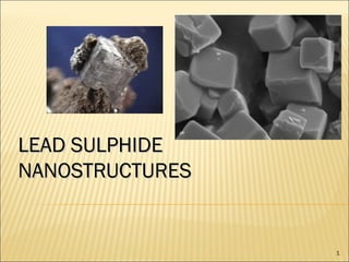
- 2. Lead(II) sulfide (PbS), most often purified from the mineral galena is a semiconductors of the II-VI family. The structure of PbS is identical to that of halite, NaCl. The two minerals have the same crystal shapes, symmetry and cleavage. Lead sulfide (PbS) is an important direct narrow - bandgap semiconductor with a bulk bandgap of 0.41 eV at 300K. The exciton Bohr radius of 18nm is relatively large compared to many semiconductors, which makes this lead chalcogenide an interesting material to study quantum effects.
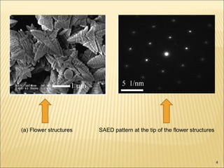
- 3. PbS flower-shaped dendritic nanostructures were prepared by the hydrothermal method. In this method, 0.05M Pb(NO3)2 and 0.1M thiourea and 3.5 g acrylamide were dissolved in 70ml of deionized (D.I.) water. The above solution was loaded into a 100-ml Teflon-lined stainless steel autoclave and heated in an oven at 160 ŌŚ”C for 12 h. The system is undisturbed till the oven reaches room temperature and the precipitate is collected washed with D.I. water 4ŌĆō5 times and dried in vacuum at 60 ŌŚ”C.
- 4. (a) Flower structures SAED pattern at the tip of the flower structures
- 5. Mixed structures of dendrites and sheets were also prepared by a similar method. Here, 0.12 g of N-cetyl-N,N,N-trimethyl-ammonium bromide (CTAB)was added to 20ml of D.I.water, then 0.08 ml CS2 was added into the above solution and thoroughly mixed at room temperature using magnetic stirrer. After CTAB dissolved completely, 1.2 ml of aqueous ammonia (NH3┬ĘH2O, 25 wt.%) was added into the clear solution, which was followed by the addition of 10 ml of 0.1Maqueous Pb(CH3COO)2. A pale yellow precipitate appeared, which was the basic acetate of lead. After stirring slowly for 5mins, the reaction temperature was increased to 40 ŌŚ”C and the system incubated at the same temperature for 3 days without disturbing it. The black precipitate was collected, washed with D.I. water, and dried in air at room temperature.
- 6. Prism shaped rod-like structures were also prepared by the hydrothermal method. Equimolar (0.1M) Pb(CH3COO)2 and Na2S2O3 were dissolved in 80ml D.I. water and the above solution was transferred to the 100-ml Teflon-lined stainless steel autoclave and maintained at 100 ŌŚ”C for 5 h. The black precipitate was collected, washed in D.I. water 5ŌĆō6 times and dried in air at 50 ŌŚ”C. It was seen that cubic shaped micro-crystals were obtained in this method at elevated temperature of about 150 ŌŚ”C.
- 7. (b)Sheet and Dendrite structures (c)Rod-like structures Cubic shaped micro-crystals
- 8. Chemical bath deposition of the flower-like PbS microstructures was also carried out . Here, equimolar solutions of (0.1M) Pb(CH3COO)2 and thiourea in methanol were prepared separately. Equal volumes of both the solutions were taken in a beaker and stirred for 5min. The beaker was covered with parafilm and left undisturbed. The solution turned brown in 15 min and after 20 min particles appeared. A black precipitate appeared at the bottom of the beaker after 6 h. The precipitate was collected, filtered, washed with methanol 5ŌĆō6 times and dried in vacuum.
- 9. (d)NanoŌĆōmicroclusters obtained by means of CBD
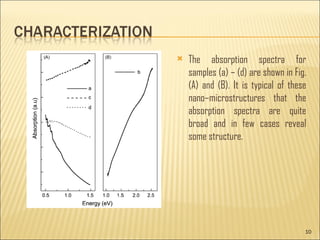
- 10. The absorption spectra for samples (a) ŌĆō (d) are shown in Fig. (A) and (B). It is typical of these nanoŌĆōmicrostructures that the absorption spectra are quite broad and in few cases reveal some structure.
- 11. But for sample (b), which has absorption extending into visible region till 2.5 eV, all the other samples have absorption in the NIR region between 0.5 and 1.5 eV. Whereas the absorption of samples (a) and (d) tends to increase towards lower energies, samples (b) and (c) exhibit the usual behavior of increasing absorption with increasing energy. The broadness of the absorption spectra indicates the size distribution. The broadness of the absorbance peaks was linked with size difference between primary and sub-branches of the dendrites, and scattering effects also need to be taken into account.
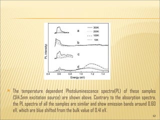
- 12. The temperature dependent Photoluminescence spectra(PL) of these samples (514.5nm excitation source) are shown above. Contrary to the absorption spectra, the PL spectra of all the samples are similar and show emission bands around 0.60 eV, which are blue shifted from the bulk value of 0.41 eV.
- 13. Though the samples have different morphologies, the luminescence band around 0.60 eV in all the samples indicate that its origin can be from the bigger sized crystallites. The temperature dependent PL spectra of 0.60 eV band exhibits similar behavior of decreasing intensity with decreasing temperature till 60ŌĆō70K. Since the surface is relatively large and plays an important role in these structures the surface passivation/deactivation helps in many ways in enhancing both optical and electrical properties of these nanoŌĆōmicrostructures. A few organic ligands get attached to the surface of the nanostructures and passivate the dangling bonds at the surface, which is called capping.
- 14. We have used mercaptoethanol, dodecanethiol, and oleic acid as capping agents to passivate the large surface of these structures. After capping, the samples have shown considerable improvement in their PL spectra as shown below.
- 15. It is noted here that the intensity of the low energy transitions is an order of magnitude smaller compared to the higher energy transitions in the first two samples. This kind of interdependent behaviour reveals the carrier transfer mechanism between different energy states of the quantum dots (from smaller particles to bigger particles). From the above results, it is inferred that the surface capping helps in suppressing some of the nonradiative paths and activates the core of the quantum dots. These results also indicate that even after capping there may be nonradiative paths available for the carriers in the bulk of the samples. From the morphology of these flower structures, we expect that the capping will be effective only to a certain extent at the surface of the microstructures, however deep inside the particulates, i.e., in the bulk of the sample, the passivation might not be effective.
- 16. Thick viscous solutions containing the PbS nano-micro structures in a conducting polymer matrix along with an organic solvent were prepared to test certain electrical behaviour. For this 0.25gm of PbS was mixed in a 1ml solution of PEG in DMF (1ml). Thin films of these solutions were deposited on p-type silicon substrate by spin coating. Electrical characterization of these films gave no particular junction characteristics and behaved almost ohmically. However on illuminating the with visible and near IR radiation the current produced increased by about 10 times.
- 17. mA mA V V With illumination Without illumination
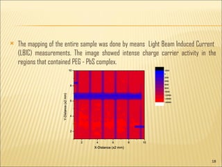
- 18. The mapping of the entire sample was done by means Light Beam Induced Current (LBIC) measurements. The image showed intense charge carrier activity in the regions that contained PEG - PbS complex.
- 19. The photoconductive activity of PbS ŌĆō PEG films promises a large number of possible applications in photonics etc These PbS nanostructures are also being used in sensors, phtodetectors etc.
- 20. Temperature and capping dependence of NIR emission from PbS nanoŌĆōmicro crystallites with different morphologies by Naresh Babu Pendyala ŌłŚ, K.S.R. Koteswara Rao. L. Dong, Y. Chu, Y. Liu, M. Li, F. Yang, L. Li, J. Colloid Interf. Sci. 301 (2006) 503. www.wikipedia.org
