ADS Lab 5 Report
ŌĆóDownload as DOCX, PDFŌĆó
0 likesŌĆó515 views

The 4-bit CPU was designed to execute 18 distinct operations from a lookup table. It was tested by executing an instruction set that performed operations like load, store, add, and jump instructions. The accumulator and program counter displays were observed after each instruction to verify the correct operations. Various components like a RAM, ALU, program counter, and decoders were used in the design. The group members demonstrated different parts of the instruction set to verify the CPU was functioning properly.
ADS Lab 5 Report
- 1. Advanced Digital Systems Dr. Megherbi Lab #5 4-bit Central Processing Unit (CPU) Due date : 11/24/15 Prepared by : Javier Guzman Edson Montrond Riddhi Shah
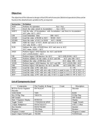
- 2. Objective: The objective of thislabwasto designa 4-but CPU whichexecutes18distinctoperations(theycanbe foundonthe attachedLook-uptable (LUT)),asrequired. Instruction Definition NOP Perform No operation Acc->Acc INV Invert the value stored in Accumulator Acc->ACC SHIFT Add the value of Accumulator with Accumulator and Store in Accumulator ACC plus ACC->ACC LDI Load Immediate Data DB->ACC LOAD Load the value of RAM to ACC RAM->ACC STORE Store the value of ACC in RAM ACC->RAM ADD ADD the values of ACC, RAM and store it in ACC ACC plus RAM -> ACC SUB Subtract the value of RAM from ACC and store in ACC ACC minus RAM-> ACC AND Perform logical AND function for ACC and RAM ACC (AND) RAM-> ACC OR Perform logical OR function for ACC ACC (OR) RAM->ACC ADDI Perform addition for the values of ACC and DB ACC plus DB->ACC SUBI Subtract the value of DB from ACC ACC minus DB -> ACC ANDI Perform logical AND function for ACC and DB ACC (AND) DB->ACC ORI Perform logical OR function for ACC and DB ACC (OR) DB-> ACC JMPZ Load the value of PC with Zero 0-> PC JIFZ Load the value of PC with zero only if ACC is equal to zero 0->PC if ACC=0 JIFN Load the value of PC with zero only if ACC is equal to 1111 0->PC if ACC=F JIFP Load the value of PC with zero only if ACC is equal to 0001 0->PC if ACC=1 List of Components Used Components Part Number & Range Count Description BCD to Seven Segment Decoder SN74LS247 2 Decoder 16X4 RAM 7489 1 RAM Hex D Flip Flop 74LS174 2 D Flip Flop DIP Switch 3 DIP Switch Dual 7 Segment Display 08TIE524 1 Display Toggle Switch 17TOGSD-M SPDT 1 Toggle Switch 2-Input Multiplexer SN54/74LS157 1 4 bit 2-1 Mux Hex Inverter SN54/74LS04 1 Inverter Resistors 220 Ohms 2 Resistor Program Counter 74LS569N 1 Program Counter Quad 2 Input NAND gate 74LS00 1 NAND Gate
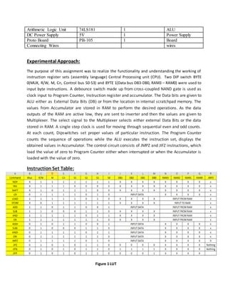
- 3. Arithmetic Logic Unit 74LS181 1 ALU DC Power Supply 5V 1 Power Supply Proto Board PB-105 1 Board Connecting Wires wires Experimental Approach: The purpose of this assignment was to realize the functionality and understanding the working of instruction register sets (assembly language) Central Processing unit (CPU). Two DIP switch BYTE 0(MUX, R/W, M, Cn, Control bus S0-S3) and BYTE 1(Data bus DB3-DB0, RAM3 ŌĆō RAM0) were used to input byte instructions. A debounce switch made up from cross-coupled NAND gate is used as clock input to Program Counter, Instruction register and accumulator. The Data bits are given to ALU either as External Data Bits (DB) or from the location in internal scratchpad memory. The values from Accumulator are stored in RAM to perform the desired operations. As the data outputs of the RAM are active low, they are sent to inverter and then the values are given to Multiplexer. The select signal to the Multiplexer selects either external Data Bits or the data stored in RAM. A single step clock is used for moving through sequential even and odd counts. At each count, Dipswitches set proper values of particular instruction. The Program Counter counts the sequence of operations while the ALU executes the instruction set, displays the obtained values in Accumulator. The control circuit consists of JMPZ and JIFZ instructions, which load the value of zero to Program Counter either when interrupted or when the Accumulator is loaded with the value of zero. Instruction Set Table: Figure 1 LUT
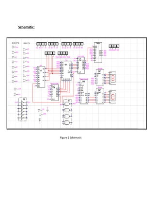
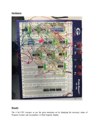
- 5. Hardware: Result: The 4 bit CPU executes as per the given instruction set by displaying the necessary values of Program Counter and Accumulator in Dual Segment Display.
- 6. Conclusion: Schematic, Simulation and Hardware Implementation of this assignment is successfully implemented and results are displayed to TA Fault Tolerance Question: 1: Execute the following instruction set in the 4 Bit CPU and make a note on each instruction. The following instruction set is executed and the required values in both Accumulator and Program Counter are observed. Instruction Accumulator Display Program Counter Display Notes: LDI 4 4 7 The value of 4 is displayed in Accumulator. STORE 10 4 8 The value of 4 is stored in 10-memory location of RAM. LDI 1 1 9 The value of 1 is displayed in Accumulator LOAD 10 4 10 The value of 4 is loaded from RAM and displayed in Accumulator. LDI 2 2 11 The value of 2 is displayed in Accumulator ADD 10 6 12 The value stored in 10 memory position of RAM is added to value of Accumulator and gets displayed in Accumulator. JIFZ 6 12 The Program Counter is same value if not clocked but if clocked then the PC changes to 13 since accumulator is not zero the value remains the same. JMPZ 6 0 The value of Program counter is set to zero. ADD I 2 8 1 The external Data bit 2 is added to Accumulator and the value is stored in Accumulator. LOAD 0 0 2 The value of zero is loaded in Accumulator JIFZ 0 0 The program counter executes the jump instruction as the value of Accumulator is zero and JIFZ instruction is set. Javier: Demonstrated the first to three instructions. Edson: Demonstrated four to seven instructions Riddhi: Demonstrated eight to eight to eleven instructions