Advanced pcb designing with or cad pcb designe in waayoo.coom
ŌĆóDownload as DOCX, PDFŌĆó
0 likesŌĆó365 views

This document provides an overview of an advanced PCB design training program covering topics such as schematic design, PCB layout, signal integrity, component orientation, generating output files, and more. The training uses Cadence's OrCAD PCB Designer and DIPTRACE software and teaches skills from building basic schematics to multi-sheet designs, component placement, routing, generating output files for fabrication, and techniques for minimizing electromagnetic interference. The program also includes six months of industrial training support and feedback.

Advanced pcb designing with or cad pcb designe in waayoo.coom
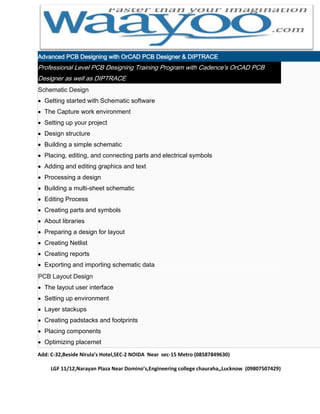
- 1. Advanced PCB Designing with OrCAD PCB Designer & DIPTRACE Professional Level PCB Designing Training Program with Cadence's OrCAD PCB Designer as well as DIPTRACE Schematic Design Getting started with Schematic software The Capture work environment Setting up your project Design structure Building a simple schematic Placing, editing, and connecting parts and electrical symbols Adding and editing graphics and text Processing a design Building a multi-sheet schematic Editing Process Creating parts and symbols About libraries Preparing a design for layout Creating Netlist Creating reports Exporting and importing schematic data PCB Layout Design The layout user interface Setting up environment Layer stackups Creating padstacks and footprints Placing components Optimizing placemet Add: C-32,Beside NirulaŌĆÖs Hotel,SEC-2 NOIDA Near sec-15 Metro (08587849630) LGF 11/12,Narayan Plaza Near DominoŌĆÖs,Engineering college chauraha,,Lucknow (09807507429)
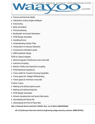
- 2. Fanout and thermal reliefs Interactive routing single-multilayer Autorouting Back annotation Post processing Bootloader and board fabrication PCB Design examples Handling Errors Understanding Gerber Files Introduction to Industry Standard Component orientation guide SMD padstack design PCB for Signal Integrity Electromagnetic Interference and cross-talk Inductive Coupling Electric Fields and Capacitive coupling PCB Electrical Impedence Trace width for Current-Carrying Capability Trace space for Voltage Withstanding Trace space to minimize cross-talk Further Topics Making and editing capture parts Making and editing footprints PCB Design Examples Artwork development and board fabrication Genertating the Route file Genertating the Pick & Place files Add: C-32,Beside NirulaŌĆÖs Hotel,SEC-2 NOIDA Near sec-15 Metro (08587849630) LGF 11/12,Narayan Plaza Near DominoŌĆÖs,Engineering college chauraha,,Lucknow (09807507429)
- 3. Six Month Industrial Training Certificate, Future Support, Feedbacks Add: C-32,Beside NirulaŌĆÖs Hotel,SEC-2 NOIDA Near sec-15 Metro (08587849630) LGF 11/12,Narayan Plaza Near DominoŌĆÖs,Engineering college chauraha,,Lucknow (09807507429)