Altium productivity
Download as ppt, pdf1 like2,249 views

This document provides 17 productivity tips for Altium Designer, including how to walk through nets to check a design, manage layer sets, use net name prefixes to set up classes, find unconnected nets, delete long traces quickly, and move selections by X and Y coordinates. It also recommends additional resources for learning more Altium Designer tips and tricks.

Altium productivity
- 1. Ten Productivity Tips For Altium Designer That Seem To Be Hidden. Carl Schattke, Sr. PCB Design Engineer, Tesla Motors, Inc. Copyright 2011 All rights reserved
- 2. 10+ Altium Designer Productivity Tips 1. How to walk through the nets in a design to check it. 2. How to manage layer sets 3. Using net name prefixes on nets to set up classes quickly. 4. How to use schematic net names to ease class definition for rules setup. 5. How to get the total match net lengths on extended nets in a few seconds. 6. How to find that last small unconnected net on a big design. 7. How to place a drill drawing stack up table with all the parameters 8. Method for how to close out test point usage errors on a large design. 9. How to tag team placement with multiple users when your not all on SVN together. 10. How to use unions and rooms to ease placement 11. How to delete a one or more long traces quickly 12. How to move stuff from one layer to another 13. How to tile your schematics and board into two panes quickly 14. How to use the layer stack manager to show placement and test point keepouts 15. How to bring a spreadsheet into Altium. 16. How to change layer names to keep track of them better 17. Move selections by X,Y 18. Edit Move Polygons 19. Microsoft tip - Use Alt-Tab to switch between open windows.
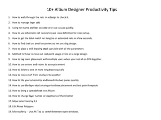
- 3. How to walk through the nets in a design to check it. 1) Open the PCB- Z,B –Zoom board 2) Open up the PCB panel – V,W,P,P – View Workspace panels, PCB, PCB 3) Select the nets pulldown 4) Select a class to see all the nets in a group – Set options to Dim or Mask, select, zoom board, clear existing . 5) Select the class <All Nets> - In the list of nets scroll up and down with up and down arrows. Each net will be highlighted. Use shift or cntl key to select multiple nets. 6) Click in PCB to turn off selection, and see nets in the current layer colors. 7) Another way - Use Edit Select component connections
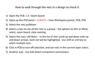
- 4. How to manage layer sets • Save favorite view options by function such as placement, All routes, planes, Drawings, etc. • Top place, bottom place, bot place flipped • LMB click on the LS button in the lower left • Select board layer sets – new set • Build a net set from current selections or pick from list. L or OL to bring up • It does not save the Show/Hide status, click SHIFT-D to bring it up. • Use these to quickly switch into desired views. • Use SHIFT-S to toggle to single layer mode. • Use N,S,A to show all design nets, use N,H,A to Hide all nets – Also use this to see nets on component N,S,O or net N,S,N
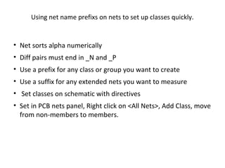
- 5. Using net name prefixs on nets to set up classes quickly. • Net sorts alpha numerically • Diff pairs must end in _N and _P • Use a prefix for any class or group you want to create • Use a suffix for any extended nets you want to measure • Set classes on schematic with directives • Set in PCB nets panel, Right click on <All Nets>, Add Class, move from non-members to members.
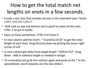
- 6. How to get the total match net lengths on xnets in a few seconds. • Create a net class that includes all nets in the extended class “D0,D0- 1,D0-2…D15,D15-1,D15-2” • Shift click on top and bottom net in panel to select all the nets. CTRL- C to put in buffer. • Open an Excel worksheet– CTRL-V to Paste in • In new column add the Xnet’s “=Sum(D12,D14)” to get the total length of each Xnet. Drag formula down by picking the lower right corner of cell. • In new column get delta from target length “=$F$12-F12” Drag down. Add or subtract length as needed in design. • To recalculate just grab the netclass again and paste at the * in the spreadsheet, you’ll instantly see the new delta’s
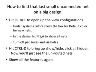
- 7. How to find that last small unconnected net on a big design. • Hit OL or L to open up the view configurations – Under systems colors check the box for Default color for new nets. – In the design hit N,S,A to show all nets – Turn off pad holes and via holes • Hit CTRL-D to bring up show/hide, click all hidden. Now you’ll just see the un-routed nets. • Show all the features again.
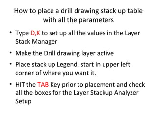
- 8. How to place a drill drawing stack up table with all the parameters • Type D,K to set up all the values in the Layer Stack Manager • Make the Drill drawing layer active • Place stack up Legend, start in upper left corner of where you want it. • HIT the TAB Key prior to placement and check all the boxes for the Layer Stackup Analyzer Setup
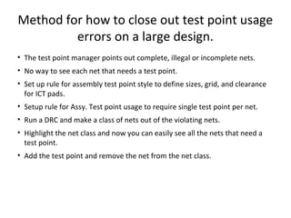
- 9. Method for how to close out test point usage errors on a large design. • The test point manager points out complete, illegal or incomplete nets. • No way to see each net that needs a test point. • Set up rule for assembly test point style to define sizes, grid, and clearance for ICT pads. • Setup rule for Assy. Test point usage to require single test point per net. • Run a DRC and make a class of nets out of the violating nets. • Highlight the net class and now you can easily see all the nets that need a test point. • Add the test point and remove the net from the net class.
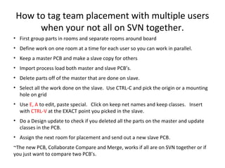
- 10. How to tag team placement with multiple users when your not all on SVN together. • First group parts in rooms and separate rooms around board • Define work on one room at a time for each user so you can work in parallel. • Keep a master PCB and make a slave copy for others • Import process load both master and slave PCB’s. • Delete parts off of the master that are done on slave. • Select all the work done on the slave. Use CTRL-C and pick the origin or a mounting hole on grid • Use E, A to edit, paste special. Click on keep net names and keep classes. Insert with CTRL-V at the EXACT point you picked in the slave. • Do a Design update to check if you deleted all the parts on the master and update classes in the PCB. • Assign the next room for placement and send out a new slave PCB. ~The new PCB, Collaborate Compare and Merge, works if all are on SVN together or if you just want to compare two PCB’s.
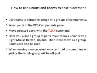
- 11. How to use unions and rooms to ease placement • Use rooms to setup the design into groups of components. • Select parts in the PCB Components panel • Move selected parts with the T,O,R command • Once you place a group of parts make them a union with a Right Mouse Button, Unions. Then it will move as a group. Rooms can also be used. • When moving a union select on a centroid or something on grid or the whole group will be off grid.
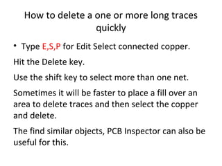
- 12. How to delete a one or more long traces quickly • Type E,S,P for Edit Select connected copper. Hit the Delete key. Use the shift key to select more than one net. Sometimes it will be faster to place a fill over an area to delete traces and then select the copper and delete. The find similar objects, PCB Inspector can also be useful for this.
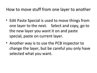
- 13. How to move stuff from one layer to another • Edit Paste Special is used to move things from one layer to the next. Select and copy, go to the new layer you want it on and paste special, paste on current layer. • Another way is to use the PCB inspector to change the layer, but be careful you only have selected what you want.
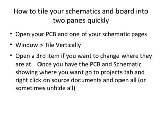
- 14. How to tile your schematics and board into two panes quickly • Open your PCB and one of your schematic pages • Window > Tile Vertically • Open a 3rd item if you want to change where they are at. Once you have the PCB and Schematic showing where you want go to projects tab and right click on source documents and open all (or sometimes unhide all)
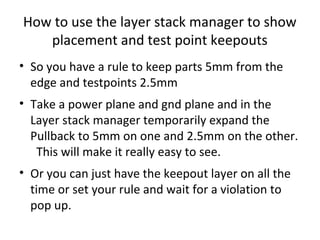
- 15. How to use the layer stack manager to show placement and test point keepouts • So you have a rule to keep parts 5mm from the edge and testpoints 2.5mm • Take a power plane and gnd plane and in the Layer stack manager temporarily expand the Pullback to 5mm on one and 2.5mm on the other. This will make it really easy to see. • Or you can just have the keepout layer on all the time or set your rule and wait for a violation to pop up.
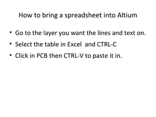
- 16. How to bring a spreadsheet into Altium • Go to the layer you want the lines and text on. • Select the table in Excel and CTRL-C • Click in PCB then CTRL-V to paste it in.
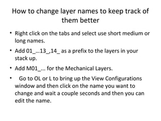
- 17. How to change layer names to keep track of them better • Right click on the tabs and select use short medium or long names. • Add 01_…13_,14_ as a prefix to the layers in your stack up. • Add M01_... for the Mechanical Layers. • Go to OL or L to bring up the View Configurations window and then click on the name you want to change and wait a couple seconds and then you can edit the name.
- 18. Move selections by X,Y • Select the stuff you want and then Edit Select move by XY Put in the exact distances you want to move the selections. • Remember you can toggle the X and Y and this might save some typing. Also the positive and negative can toggle.
- 19. Edit Move Polygons • Edit > Move > Polygon Vertices • Use EMG for short cut.
- 20. Microsoft tips - Use Alt-Tab to switch between open windows. • Use Alt-Tab to switch between open windows. • Use CTRL-ALT-PRINT SCREEN to copy image • Use CTRL Arrows to jump by words not letters • Use CNTL-ALT-DEL > Task manager > Process> View> Select Columns - to see if program is dead look at I/O reads & writes and usage.
- 21. More Productivity tips!!! • Altium Learning Guides: http://www.altium.com/community/learning-guides/en/learning-guides_home.cfm# • Scripts in Altium Designer: http://www.altium.com/files/pdfs/Increaseyourproductivity.pdf • 52 Time Saving Windows Tips: http://vitamincm.com/windows-shortcuts-tips/ • Johns Blog Altium Designer tips: http://www.johnstowers.co.nz/blog/index.php/reference/altium-designer-tips/ • Blackstick Altium Tips: http://www.blackstick.co.uk/blog/?tag=altium-tips • Bluechip Highspeed Tips: http://fplreflib.findlay.co.uk/articles/37941/HiSpeedDesignTutorialforAltiumDesigner_long.pdf • Altium Twitter: http://twitter.com/#!/altium • Altium Live Videos: http://altiumvideos.live.altium.com/#Detail/1026 • Click on a button you never did before and see what it does! Carl Schattke can be contacted at carl@schattke.org or at 888-204-3704