Application Report On Stellaris To DAC7311 (Spi)
- 1. Interfacing Stellaris to DAC (SPI) Stellaris LM3S811 EVM to DAC7311 Data Converter EVM Abstract The DAC7311 is low power, single channel, voltage output digital-to-analog 12-bits converters (DAC). It is monotonic by design and provides excellent linearity and minimizes undesired code-to-code transient voltage. By interfacing the DAC7311 with Stellaris LM3S811 through SPI, we can increase the range of suitable application for Stellaris to another level. Related code and additional information are provided. Contents 1. Introduction 2 2. Stellaris LM3S811 Synchronous Serial Interface (SSI) 2 2.1 Frame Format 2 2.2 Evaluation board layout & Connection 4 3. DAC7311 EVM 6 3.1 Pin Configuration 6 3.2 Digital Interface 6 3.3 Power Supplies 7 3.4 Default Jumper Location 7 3.5 Actual DAC7311 Snapshot 8 4. Establish communication between Stellaris and DAC7311 9 4.1 Functions used in demo code 10 5. Reference 14 Interfacing Stellaris LM3S811 with DAC7311 Page 1 of 14 25/5/2011
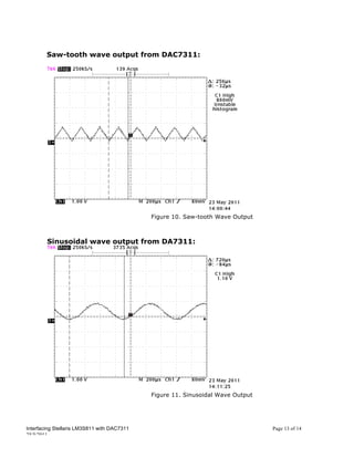
- 2. 1. Introduction This application report will enhance the already feature-rich Stellaris LM3S811 microcontroller with DAC capability using DAC7311 through SPI. The demo code will generate square wave, saw-tooth wave or Sinusoidal wave from the DAC7311 output. It offers the customer an easy solution and will definitely shorten the development process. 2. Stellaris LM3S811 Synchronous Serial Interface (SSI) The Stellaris Synchronous Serial Interface (SSI) is a master or slave interface for synchronous serial communication with peripheral devices that have either Freescale SPI, MICROWIRE, or Texas Instruments synchronous serial interface. In the demo code, we will be using the Freescale SPI format. The Stellaris SSI module has the following features: • Master or slave operation • Programmable clock bit rate and prescale • Separate transmit and receive FIFOs, 16 bits wide, 8 locations deep • Programmable interface operation for Freescale SPI, MICROWAVE, or Texas Instruments synchronous serial interfaces • Programmable data frame size for 4 to 16 bits • Internal loopback test mode for diagnostic/debug testing *The information on Stellaris LM3S811 SPI is mostly taken from Stellaris LM3SS811 Datasheet. The information provided above and below should be enough to understand and use the SPI feature. For more information, please refer to section 12, page 400 from the datasheet. 2.1 Frame Format To interface with the DAC7311, the Freescale SPI frame type will be chosen. The Freescale SPI interface is a four-wire interface where the SSIFss signal behaves as a slave select. The main feature of the Freescale SPI format is that the inactive state and phase of the SSIClk signal are programmable through the SPO and SPH bits within the SSISCR0 control register. SPO Clock Polarity Bit: When the SPO clock polarity control bit is low, it produces a steady state low value on the SSIClk pin. If the SPO is high, a steady state high Interfacing Stellaris LM3S811 with DAC7311 Page 2 of 14 25/5/2011
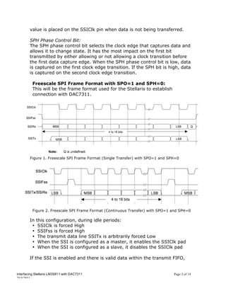
- 3. value is placed on the SSIClk pin when data is not being transferred. SPH Phase Control Bit: The SPH phase control bit selects the clock edge that captures data and allows it to change state. It has the most impact on the first bit transmitted by either allowing or not allowing a clock transition before the first data capture edge. When the SPH phase control bit is low, data is captured on the first clock edge transition. If the SPH bit is high, data is captured on the second clock edge transition. Freescale SPI Frame Format with SPO=1 and SPH=0: This will be the frame format used for the Stellaris to establish connection with DAC7311. Figure 1. Freescale SPI Frame Format (Single Transfer) with SPO=1 and SPH=0 Figure 2. Freescale SPI Frame Format (Continuous Transfer) with SPO=1 and SPH=0 In this configuration, during idle periods: • SSIClk is forced High • SSIFss is forced High • The transmit data line SSITx is arbitrarily forced Low • When the SSI is configured as a master, it enables the SSIClk pad • When the SSI is configured as a slave, it disables the SSIClk pad If the SSI is enabled and there is valid data within the transmit FIFO, Interfacing Stellaris LM3S811 with DAC7311 Page 3 of 14 25/5/2011
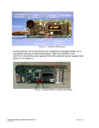
- 4. the start of transmission is signified by the SSIFss master signal being driven Low, which causes slave data to be immediately transferred onto the SSIRx line of the master. The master SSITx output pad is enabled. One half period later, valid master data is transferred to the SSITx line. Now that both the master and slave data have been set, the SSIClk master clock pin becomes Low after one further half SSIClk period. This means that data is captured on the falling edges and propagated on the rising edges of the SSIClk signal. In the case of a single word transmission, after all bits of the data word are transferred, the SSIFss line is returned to its idle High state one SSIClk period after the last bit has been captured. However, in the case of continuous back-to-back transmissions, the SSIFss signal must be pulsed high between each data word transfer. This is because the slave select pin freezes the data in its serial peripheral register and does not allow it to be altered if the SPH bit is logic zero. Therefore, the master device must raise the SSIFss pin of the slave device between each data transfer to enable the serial peripheral data write. On completion of the continuous transfer, the SSIFss pin is returned to its idle state one SSIClk period after the last bit has been captured. 2.2 Evaluation Board Layout & Connections To use the SPI function, need to connect SCLK, SFSS and STx to the DAC7311. SCLK, SFSS and STx are highlighted as red in picture 1 on page 5. Interfacing Stellaris LM3S811 with DAC7311 Page 4 of 14 25/5/2011
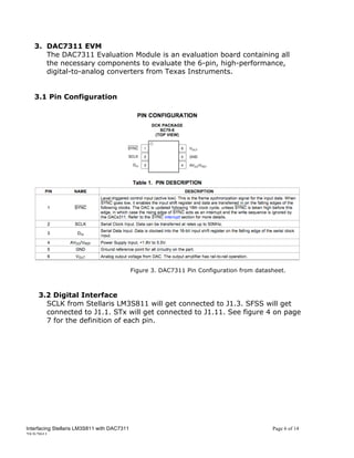
- 5. Picture 1. LM3S811 EVM Layout During testing, the actual device pin snapshot is provided below. It is connected exactly as mentioned above. Both the LM3S811 and DAC7311 shared the same ground from the external power supply (See picture 2 on page 5). Picture 2. Actual LM3S811 used during testing Interfacing Stellaris LM3S811 with DAC7311 Page 5 of 14 25/5/2011
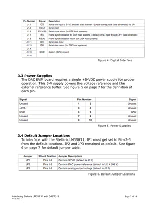
- 6. 3. DAC7311 EVM The DAC7311 Evaluation Module is an evaluation board containing all the necessary components to evaluate the 6-pin, high-performance, digital-to-analog converters from Texas Instruments. 3.1 Pin Configuration Figure 3. DAC7311 Pin Configuration from datasheet. 3.2 Digital Interface SCLK from Stellaris LM3S811 will get connected to J1.3. SFSS will get connected to J1.1. STx will get connected to J1.11. See figure 4 on page 7 for the definition of each pin. Interfacing Stellaris LM3S811 with DAC7311 Page 6 of 14 25/5/2011
- 7. Figure 4. Digital Interface 3.3 Power Supplies The DAC EVM board requires a single +5-VDC power supply for proper operation. This 5-V supply powers the voltage reference and the external reference buffer. See figure 5 on page 7 for the definition of each pin. Figure 5. Power Supplies 3.4 Default Jumper Locations To interface with the Stellaris LM3S811, JP1 must get set to Pins2-3 from the default locations. JP2 and JP3 remained as default. See figure 6 on page 7 for default jumper table. Figure 6. Default Jumper Locations Interfacing Stellaris LM3S811 with DAC7311 Page 7 of 14 25/5/2011
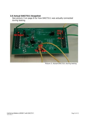
- 8. 3.5 Actual DAC7311 Snapshot See picture 3 on page 8 for how DAC7311 was actually connected during testing. Picture 3. Actual DAC7311 during testing Interfacing Stellaris LM3S811 with DAC7311 Page 8 of 14 25/5/2011
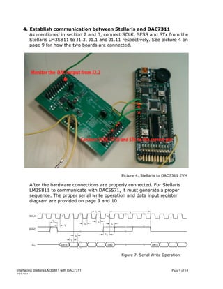
- 9. 4. Establish communication between Stellaris and DAC7311 As mentioned in section 2 and 3, connect SCLK, SFSS and STx from the Stellaris LM3S811 to J1.3, J1.1 and J1.11 respectively. See picture 4 on page 9 for how the two boards are connected. Picture 4. Stellaris to DAC7311 EVM After the hardware connections are properly connected. For Stellaris LM3S811 to communicate with DAC5571, it must generate a proper sequence. The proper serial write operation and data input register diagram are provided on page 9 and 10. Figure 7. Serial Write Operation Interfacing Stellaris LM3S811 with DAC7311 Page 9 of 14 25/5/2011
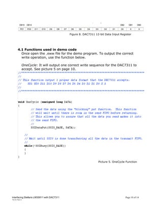
- 10. Figure 8. DAC7311 12-bit Data Input Register 4.1 Functions used in demo code Once open the .eww file for the demo program. To output the correct write operation, use the function below. OneCycle: It will output one correct write sequence for the DAC7311 to accept. See picture 5 on page 10. Picture 5. OneCycle Function Interfacing Stellaris LM3S811 with DAC7311 Page 10 of 14 25/5/2011
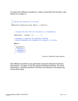
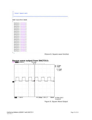
- 11. To output the different waveforms, simply uncomment the function. See picture 6 on page 11. Picture 6. Different output options. The different waveforms are generated using the OneCycle functions. See picture 7 on page 12 for the square waveform function. For more information, all these waveform functions are defined in the beginning of the demo code. Interfacing Stellaris LM3S811 with DAC7311 Page 11 of 14 25/5/2011
- 12. Picture 8. Square wave function Square wave output from DAC7311: Figure 9. Square Wave Output Interfacing Stellaris LM3S811 with DAC7311 Page 12 of 14 25/5/2011
- 13. Saw-tooth wave output from DAC7311: Figure 10. Saw-tooth Wave Output Sinusoidal wave output from DA7311: Figure 11. Sinusoidal Wave Output Interfacing Stellaris LM3S811 with DAC7311 Page 13 of 14 25/5/2011
- 14. 5. Reference Stellaris LM3S811 Microcontroller Datasheet (DS-LM3S811-9102) Stellaris LM3S811 Evaluation Board User’s Manual (EK-LM3S811-01) DAC7311 Datasheet (SBAS442) SC70 DAC EVM User’s Guide (SLAU299) Interfacing Stellaris LM3S811 with DAC7311 Page 14 of 14 25/5/2011

