Audio amplifier
- 2. Project Report Audio Amplifier Department of Electrical Engineering Sukkur IBA By: Zeeshan Ahmed 033-14-0062 Raheel Nadeem 033-14-0074 Shahryar Prepared for Sir Engr. Afaque Manzoor Soomro July 20,2016
- 3. Abstract A bipolar junction transistor is a semiconductor device used to amplify or switch electronic signals. The device is a solid piece of semiconductor material with three connection terminal. The purpose of this project is to design, build, and study the operation of a multistage amplifier. We will accomplish this by using a Common Emitter amplifier. There are multiple stages because a single stage may not be sufficient for most applications. Two big advantages of multistage over single stage are that it has a higher gain, and has flexibility for higher input and output impedances. Thatâs why itâs chosen as a major project.
- 4. Table of Contents IntroductionâĶâĶâĶâĶâĶâĶâĶâĶâĶâĶâĶâĶâĶâĶâĶâĶâĶâĶâĶâĶâĶâĶ... 4 OperationâĶâĶâĶâĶâĶâĶâĶâĶâĶâĶâĶâĶâĶâĶâĶâĶâĶâĶâĶâĶâĶâĶâĶ. 5 IllustrationâĶâĶâĶâĶâĶâĶâĶâĶâĶâĶâĶâĶâĶâĶâĶâĶâĶâĶâĶâĶâĶâĶ.... 6 Common EmitterâĶâĶâĶâĶâĶâĶâĶâĶâĶâĶâĶâĶâĶâĶâĶâĶâĶâĶâĶâĶâĶâĶâĶâĶâĶâĶâĶ. 7 SimulationâĶâĶâĶâĶâĶâĶâĶâĶâĶâĶâĶâĶâĶâĶâĶâĶâĶâĶâĶâĶ............ 09 ImplementationâĶâĶâĶâĶâĶâĶâĶâĶâĶâĶâĶâĶâĶâĶâĶâĶâĶâĶâĶâĶ.... 10 ConclusionâĶâĶâĶâĶâĶâĶâĶâĶâĶâĶâĶâĶâĶâĶâĶâĶâĶâĶâĶâĶâĶâĶâĶ 11 ReferencesâĶâĶâĶâĶâĶâĶâĶâĶâĶâĶâĶâĶâĶâĶâĶâĶâĶâĶâĶâĶâĶâĶâĶ 12 âĶâĶâĶâĶâĶâĶâĶâĶâĶâĶâĶâĶâĶâĶâĶâĶâĶâĶâĶâĶâĶâĶâĶâĶâĶâĶâĶâĶâĶ..
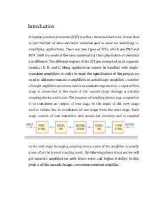
- 5. Introduction A bipolar junction transistor (BJT) is a three terminal electronic device that is constructed of semiconductor material and is used for switching or amplifying applications. There are two types of BJTs, which are PNP and NPN. Both are made of the same material but their physical characteristics are different. The different regions of the BJT are connected to its separate terminal E, B, and C. Many applications cannot be handled with single- transistor amplifiers in order to meet the specification of the project we need to add more transistor amplifiers, in a multistage amplifier, a number of single amplifiers are connected in cascade arrangement i.e. output of first stage is connected to the input of the second stage through a suitable coupling device and so on. The purpose of coupling device (e.g. a capacitor is to transform ac. output of one stage to the input of the next stage and to isolate the dc conditions of one stage from the next stage. Each stage consist of one transistor and associated circuitry and is coupled to the next stage through a coupling device name of the amplifier is usually given after the type of coupling used. By following above structure we will get accurate amplification with lower noise and higher stability. In this project all the cascaded stages are common emitter amplifier.
- 6. Operation The operation begins with analysis of common emitter amplifier with voltage-divider bias and coupling capacitors C1 and C3 on the input and output and a bypass capacitor, C2, from emitter to ground. The analysis should be of both dc and ac .it will help us to set the resistors and capacitors values and particular operating point to achieve accurate amplification. In that the input signal, Vin, is capacitively coupled to the base terminal, the output signal, Vout, is capacitively coupled from the collector to the load. The amplified output is 180° out of phase with the input. Because the ac signal is applied to the base terminal as the input and taken from the collector terminal as the output the emitter is common to both the input and output signals. There is no signal at the emitter because the bypass capacitor effectively shorts the emitter to ground at the signal frequency. All amplifiers have a combination of both ac and dc operation, which must be considered, but keep in mind that our focus is on common-emitter amplifier. Moreover, the output signal is out of phase with the input signal. As the input signal voltage changes, it causes the ac base current to change, resulting in a change in the collector current from its Q-point value. If the base current increases, the collector current increases above its Q-point value, causing an increase in the voltage drop across RC. This increase in the voltage across RC means that the voltage at the collector decreases from its Q-point. So, any change in input signal voltage results in an opposite change in collector signal voltage, which is a phase inversion
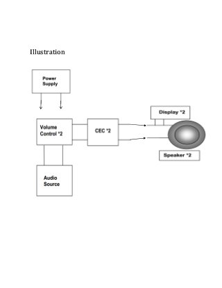
- 7. Illustration
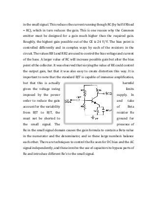
- 8. This is the main source of audio amplifier which amplifies the small signal given in form of sound. there are many types but this amplifier is chosen because this circuit has large voltage gain and large current gain, the concept behind this is to amplify small variations of current input into the base terminal. IB is increased by an input voltage variation and this current is amplified by a factor beta in IC (the current flowing into the Collector terminal), the connection to the collector terminal has resistance in series so when current increases into C there is voltage drop at C and vice versa. Biasing of the Common emitter is the design work for this stage. It is required that the BJT always stay in forward active mode, meaning that the voltage in the collector is always higher than that of the base which in turn must be higher than that at the emitter terminal. For undistorted amplification, this relationship must remain true up to the highest and lowest peaks of the output. Since there is a single voltage source of 12V, maximum amplification can occur with 12V peak to peak, providing 6V peaks from a bias point of 6V. Additionally, when the base voltage increases slightly (from input), the collector voltage will be at its minimum, meaning that peaks will create the absolute worst case for maintaining forward active mode. There is a single voltage source (in this case +12V DC) with which to create the bias, and the balance is adjusted with values of the resistors RB1, RB2, RC, and RE. The source and load resistances connected to the Common emitter do not affect its operation because they are coupled to it with capacitors, which act as open circuits to DC values and short circuits to signals with high enough frequency. This phenomenon comes about from the equation for impedance of a capacitor, Z = 1 / jwC. As can be seen, impedance is reduced by a high frequency w and by a high capacitance C. In order to create a minimal resistance for the inputs and outputs of the circuit for the entire frequency range, it is necessary to use as high a capacitance value as possible. Note that the load resistance does greatly affect the gain of the CE by acting as a resistance to ground in parallel with RC Common Emitter Amplifier
- 9. in the small signal. This reduces the current running though RC (by half if Rload = RC), which in turn reduces the gain. This is one reason why the Common emitter must be designed for a gain much higher than the required gain. Roughly, the highest gain possible out of the CE is 24 V/V. The bias point is controlled differently and in complex ways by each of the resistors in the circuit. The values RB1 and RB2 are used to control the bias voltage and current of the base. A larger value of RC will increase possible gain but alter the bias point of the collector. It was observed that varying the value of RE could control the output gain, but that it was also easy to create distortion this way. It is important to note that the standard BJT is capable of immense amplification, but that this is actually harmful given the voltage swing limits imposed by the power supply. In order to reduce the gain and take account for the variability of Beta from BJT to BJT, the resistor Re must not be shorted to ground for the small signal. The presence of Re in the small signal domain causes the gain formula to contain a Beta value in the numerator and the denominator, and so these large numbers balance each other. There are techniques to control the Re seen for DC bias and the AC signal independently, and these involve the use of capacitors to bypass parts of Re and introduce different Reâs to the small signal.
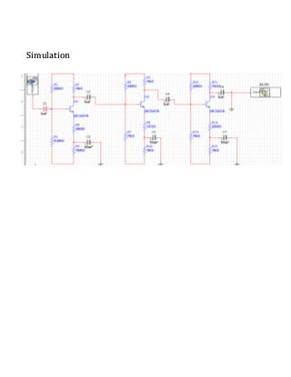
- 10. Simulation
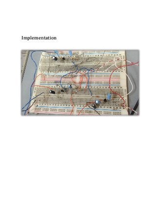
- 11. Implementation
- 12. A multistage amplifier is more useful than a single stage amplifier in that it has a higher gain and has more flexibility for higher input and output impedances. A single npn BJT was used to drive this common emitter amplifier. The collector current entering the npn BJT will be the current source driving the common emitter amplifier. Clipping occurs when the amplifier tries to output a higher power than what the amplifier can achieve. It was also tough finding a good frequency to achieve a non-noisy input. Conclusion
- 13. References www.google.com www.wikipedia.com www.pearsonhighered.com Electronic circuit devices by Floyd Principles of electronics by V.K Mehta


