際際滷

際際滷Share a Scribd company logo
Device Physics
The Diode
The Transistor
Signals
Basic Circuits
An Introduction to Basic Electronics
Debapratim Ghosh
deba21pratim@gmail.com
Electronic Systems Group
Department of Electrical Engineering
IIT Bombay
Debapratim Ghosh An Introduction to Basic Electronics 1/25
Device Physics
The Diode
The Transistor
Signals
Basic Circuits
Basic Devices
Energy Bands
Charge Carriers
Extrinsic Semiconductors
Energy Levels
Basic Electronic Devices
There are three basic devices which shape up the working and design of all electronic
circuits. They are:
Resistor- A resistor works as per Ohms Law. If V is the voltage across the resistor,
I is the current through it and R is the resistance value, then V = IR.
Capacitor- A capacitor is used to store energy in its electric field. It does not have a
linear I-V relationship, unlike a resistor.
V =
1
C
Z
I.dt
Inductor- An inductor is used to store energy in its magnetic field. Its behaviour is
somewhat analogous to a capacitor, due to its I-V relationship.
I =
1
L
Z
V .dt
+ -
V
R
I I C
+ -
V
I
+ -
V
L
Debapratim Ghosh An Introduction to Basic Electronics 2/25
Device Physics
The Diode
The Transistor
Signals
Basic Circuits
Basic Devices
Energy Bands
Charge Carriers
Extrinsic Semiconductors
Energy Levels
Semiconductor Devices- The Concept of Energy Bands
Electronic circuits are different from electrical circuits. Electronics depend on the
use of semiconductors as well e.g. Silicon, Germanium.
Semiconductors have electrical conductivity between that of conductors and
insulators.
Every element has energy levels which its electrons can occupy. A range of energy
levels which cause some common properties is called an energy band.
We consider two energy bands- the valence band (VB) and the conduction band
(CB). The valence electrons occupy the energy levels in the VB.
Debapratim Ghosh An Introduction to Basic Electronics 3/25
Device Physics
The Diode
The Transistor
Signals
Basic Circuits
Basic Devices
Energy Bands
Charge Carriers
Extrinsic Semiconductors
Energy Levels
The Concept of Energy Bands (contd...)
What does this imply? From the band structure figure, it is clear that even at room
temperature, metals have free electrons in the conduction band, which make
them good conductors.
The difference between the lowest energy level in the CB and the highest energy
level in the VB is called a band-gap. Larger the band-gap, lesser is the conductivity.
Semiconductors are insulators at room temperature. However, with an externally
applied voltage, the valence electrons in the semiconductor may overcome the
band-gap and climb to the CB. The band-gap is about 1.1 eV for silicon.
Debapratim Ghosh An Introduction to Basic Electronics 4/25
Device Physics
The Diode
The Transistor
Signals
Basic Circuits
Basic Devices
Energy Bands
Charge Carriers
Extrinsic Semiconductors
Energy Levels
Electrons and Holes
In pure silicon, the presence four valence electrons is the reason to forming a matrix
of silicon atoms in a crystalline structure. This property is called catenation.
All electrons form a part of the covalent bonds hence there are no free charge
carriers at room temperature.
However, an external electric field may cause some electrons to break the covalent
bonds and flow as a mobile charge (overcoming the band-gap). An electron
deficiency in the crystal is called a hole.
What can be said about the concentration of free electrons and holes in a pure
semiconductor?
Pure semiconductors are also called intrinsic semiconductors.
Debapratim Ghosh An Introduction to Basic Electronics 5/25
Device Physics
The Diode
The Transistor
Signals
Basic Circuits
Basic Devices
Energy Bands
Charge Carriers
Extrinsic Semiconductors
Energy Levels
Increasing the Carrier Concentration
To increase free electrons at room temperature, impurities can be introduced into
the crystal. By diffusing pentavalent element atoms (e.g. phosphorous, arsenic),
excess free electrons are created.
Such kind of semiconductors are called extrinsic semiconductors.
This process is called doping. Pentavalent dopants introduce donor atoms in the
crystal. Since electrons form the majority of carriers, this material is called an n-type
semiconductor.
Can you guess what kind of elements need to be doped into silicon to form a p-type
semiconductor? What will be the majority carriers here?
Debapratim Ghosh An Introduction to Basic Electronics 6/25
Device Physics
The Diode
The Transistor
Signals
Basic Circuits
Basic Devices
Energy Bands
Charge Carriers
Extrinsic Semiconductors
Energy Levels
Energy Levels in Semiconductors
Every crystalline solid has a characteristic energy level called the Fermi Level. It is a
hypothetical level which indicates a 50% probability of being occupied by an electron.
Why hypothetical? Consider the case of pure silicon. It has a band-gap of 1.1 eV,
indicating that the Fermi Level at 0K is exactly half-way, i.e. 0.55 eV from both CB
and VB.
The 0.55 eV energy level lies inside the band-gap, which no electron can occupy!
Hence, it is only a hypothetical measure.
Energy band diagram in (i) p- and (ii) n-type semiconductor
Debapratim Ghosh An Introduction to Basic Electronics 7/25
Device Physics
The Diode
The Transistor
Signals
Basic Circuits
p-n Junctions
Biasing Methods
The p-n Junction under Equilibrium
Fusing together a p- and an n-type semiconductor results in formation of a p-n
junction diode.
Due to large difference in carrier concentration, the electrons from the n-side tend to
diffuse to the p-side, leaving behind positively charged donor atoms behind.
Likewise, the holes start moving from the p-side, leaving behind negatively charged
acceptor atoms.
As the electrons flow into the p-side, the negatively charged acceptor ions start
repelling them (similarly with holes flowing to the n-side). This diffusion process
continues until the ionized atoms at the junction repel flow of any more carriers
across the junction.
Hence, a depletion region (devoid of charge carriers) gets formed on either side of
the junction, with a built-in potential.
Debapratim Ghosh An Introduction to Basic Electronics 8/25
Device Physics
The Diode
The Transistor
Signals
Basic Circuits
p-n Junctions
Biasing Methods
The Built-in Potential
Consider a p-n junction formed with donor doping concentration ND , acceptor doping
concentration NA and an intrinsic carrier concentration ni . If the number of mobile
carriers are n and p for electrons and holes, then as per the Law of Mass Action, we have
n2
i = n.p
We know that the Fermi Levels in n-type (Ef ,n) and p-type (Ef ,p) semiconductors are
different. The built-in junction potential is equivalent to the difference in the Fermi
Levels. We have,
Ef ,n = kT ln(
ND
ni
) Ef ,p = kT ln(
ni
NA
)
where k is the Boltzmann constant and T is the temperature in Kelvin. But, electric
potential  = E/q, where q is the electron charge. Then the built-in potential V粒 is
V粒 =
Ef ,n  Ef ,p
q
=
kT
q
ln(
NAND
n2
i
)
Exercise: Calculate the built-in potential of a silicon diode with ni = 1010
/cm3
,
ND = 1016
/cm3
and NA = 1015
/cm3
at room temperature 27
C. Vary ni , ND and NA to
study how V粒 varies.
Debapratim Ghosh An Introduction to Basic Electronics 9/25
Device Physics
The Diode
The Transistor
Signals
Basic Circuits
p-n Junctions
Biasing Methods
Diode Biasing
The following figure shows a forward-biased diode. Note that, the anode of the supply is
connected to that of the diode, and similar for the cathodes.
+
 R
+ -
VD
ID
VS
The current through the diode ID is given by Shockleys equation
ID = IS (e
VD
VT  1)
Here, VD is the voltage across the diode, VT = kT/q and Is is the reverse saturation
current.
The equation indicates that when VD increases, the diode current increases
exponentially. When 0 < VD  VT , the current is negligibly small.
When VD is negative (reverse-bias), the current is negative, but of small value.
If the reverse bias voltage is increased, the diode may break down, causing a large
reverse bias current. Shockleys equation does not hold in this region.
Debapratim Ghosh An Introduction to Basic Electronics 10/25
Device Physics
The Diode
The Transistor
Signals
Basic Circuits
p-n Junctions
Biasing Methods
What happens during forward bias?
The majority carriers (holes in p-type and electrons in n-type) are pushed towards
the junction due to the externally applied voltage.
At the p-n junction, there are two opposing electric fields acting. One is the built-in
field across the junction and the other is the influence of the externally applied
voltage.
The result is that the net field is less than the equilibrium field value, hence the
electrons from the n-side move to the p-side, resulting in a forward-bias current.
The conventional current direction is always opposite to that of the flow of
electrons, hence the forward current is from the anode (p) to the cathode (n).
As evident from Shockleys equation, the current increases with increase in VD . This
is assuming that VD < V粒. Since the electric field in the diode is strongest at the
junction, nearly all of the applied voltage is seen at the junction itself.
Exercise: Work out what happens during reverse bias. Why is the current low? Why
does breakdown occur?
Debapratim Ghosh An Introduction to Basic Electronics 11/25
Device Physics
The Diode
The Transistor
Signals
Basic Circuits
Basics of the BJT
BJT Working Principle
Revision Quiz
The Bipolar Junction Transistor (BJT)
The BJT has two p-n junctions.
Since the BJT has two junctions, it can be a p-n-p or an n-p-n device.
The three terminals are named Emitter (E), Base (B) and Collector (C).
Usually, the emitter is highly doped, the base is lightly doped (and narrow in size)
and the collector is moderately doped.
The BJT has three regions of operation, based on the biasing of the two junctions.
* Cutoff region- Here, the B-E junction is reverse biased, irrespective of the C-B junction.
* Forward-active region- Here, the B-E junction is forward biased, and the C-B junction
is reverse biased. This is the most commonly used region of operation.
* Saturation region- Here, both B-E and C-B junctions are forward biased.
C E E C
B B
Symbols for (i) NPN and (ii) PNP transistor
Debapratim Ghosh An Introduction to Basic Electronics 12/25
Device Physics
The Diode
The Transistor
Signals
Basic Circuits
Basics of the BJT
BJT Working Principle
Revision Quiz
Example- Working of a PNP transistor
Consider the figure shown below. The transistor is in forward-active region.
+

+

R1 R2
VEE VCC
As the B-E junction is forward biased, holes move across to the base (emitter
current). Since the base is narrow and lightly doped, the minority electron-hole
recombinations are less.
Due to the large carrier concentration gradient in the B-E region, majority of the
holes diffuse across the base into the C-B junction.
Since the C-B junction is reverse biased, the junction electric field sweeps out the
holes into the collector (collector current).
A small minority of electrons flow from the base to the emitter. Also, a small
number of holes coming from the emitter recombine with electrons in the base. New
electrons from the supply flow into the base to replace the the lost electrons. These
two components form the base current.
Debapratim Ghosh An Introduction to Basic Electronics 13/25
Device Physics
The Diode
The Transistor
Signals
Basic Circuits
Basics of the BJT
BJT Working Principle
Revision Quiz
Transistor Currents
Shown in the figure below are the emitter (IE ), base (IB ) and collector (IC ) currents and
their directions. These are inferred from the discussions in the previous slide.
+

+

+ - + -
VEE VCC
R1 R2
IE
IB
IC
This also gives us an idea why transistors symbols are the way they are! The following
relationships are valid for a BJT.
IE = IB + IC As a consequence of Kirchhoffs Current Law
IC
IB
= 硫 硫 is defined as the common-emitter current gain.
IC
IE
= 留 留 is defined as the common-base current gain.
Debapratim Ghosh An Introduction to Basic Electronics 14/25
Device Physics
The Diode
The Transistor
Signals
Basic Circuits
Basics of the BJT
BJT Working Principle
Revision Quiz
A Quick Quiz- and an Exercise!
Based on what weve learnt so far, try to answer these questions.
1. What are the possible values 留 can take?
2. Would we like 硫 to be large or small? Why?
3. Mentally, try to find out a relation between 留 and 硫.
4. Suggest some applications of diodes.
Exercise 1: Similar to the way we worked out for a PNP transistor, familiarize yourself
with the working of an NPN transistor.
Exercise 2: Find out what happens in the saturation region. Do the above current
relations still hold?
Debapratim Ghosh An Introduction to Basic Electronics 15/25
Device Physics
The Diode
The Transistor
Signals
Basic Circuits
Definitions and Properties
Frequency Components
Introduction to Signals
A signal is a time-dependent piece of information. It is something that removes
uncertainty in some manner.
In electronics we use two kinds of signals- voltage and current. We will mostly be
working with voltages.
Let us look at some properties of signals.
Periodicity- If x(t) is a signal and x(t + T) = x(t)  t, then x(t) is said to be
periodic with period T.
Continuity- If a signal has a defined value at all points in time, it is a
continuous-time (CT) signal. Else, it is a discrete-time (DT) signal.
There are several other signal properties- determinism, causality, energy/power
properties.
Debapratim Ghosh An Introduction to Basic Electronics 16/25
Device Physics
The Diode
The Transistor
Signals
Basic Circuits
Definitions and Properties
Frequency Components
Frequency Components of Signals
Lets answer this simple question. Consider a signal x(t) as shown.
t
x(t)
A
t0 3t0 5t0 7t0
Q: What is the frequency of x(t)?
Debapratim Ghosh An Introduction to Basic Electronics 17/25
Device Physics
The Diode
The Transistor
Signals
Basic Circuits
Definitions and Properties
Frequency Components
Frequency Components of Signals
Lets answer this simple question. Consider a signal x(t) as shown.
t
x(t)
A
t0 3t0 5t0 7t0
Q: What is the frequency of x(t)?
A: Looks simple- 1/2t0, isnt it? But not entirely! Let us see why.
Debapratim Ghosh An Introduction to Basic Electronics 17/25
Device Physics
The Diode
The Transistor
Signals
Basic Circuits
Definitions and Properties
Frequency Components
Frequency Components of Signals (contd...)
x(t) actually has infinite number of frequencies! Fourier analysis tells us how many
frequency components are present in a signal. Any periodic signal is expressed as a
superposition of finite or infinite number of frequencies, which are integral multiples
of a fundamental frequency. x(t) has a fundamental frequency of 1/2t0.
So the next question is, which signal comprises of a single frequency? The answer is
a sine wave. Recall the equation for a sine wave
x(t) = A sin(2f0t)
Sine waves form a basis for the Fourier analysis (and for every signal!).
Lets revisit some complex number mathematics. Using Eulers entity, x(t) can be
represented as
x(t) = A
ej2f0t
 ej2f0t
2j
Each exponential term is a Fourier coefficient. The frequency of each component is given
by the power. Thus, mathematically, a sine wave has two frequencies!
Debapratim Ghosh An Introduction to Basic Electronics 18/25
Device Physics
The Diode
The Transistor
Signals
Basic Circuits
Definitions and Properties
Frequency Components
Frequency Components of Signals (contd...)
Magnitude
f
0 f0
-f0
A/2
-A/2
Debapratim Ghosh An Introduction to Basic Electronics 19/25
Device Physics
The Diode
The Transistor
Signals
Basic Circuits
Basic Filters
Revision Quiz
Topics for Self Study
Introduction to Basic Filters
Based on what we have learnt about signals and basic electronic devices, we will now
study filters.
A filter is a frequency-selective circuit. This means the filter will behave differently
at different frequencies.
One which passes low frequencies but rejects high frequencies is called a low-pass
filter. Now you know what a high-pass filter is!
One which rejects high and low frequencies but passes only a certain range of
frequencies is called a band-pass filter. Now you know what a band-stop filter is!
Consider the case of a low-pass filter. How low frequencies will it pass, and how high
frequencies will it reject? The answer is through a parameter called the cut-off
frequency.
Let us see a simple example.
Debapratim Ghosh An Introduction to Basic Electronics 20/25
Device Physics
The Diode
The Transistor
Signals
Basic Circuits
Basic Filters
Revision Quiz
Topics for Self Study
A Simple Low-pass Filter
Consider the simple circuit shown below. VS is an AC source with variable frequency.
R
C
Vs Vout
The resistance of R does not vary with frequency. However, the reactance XC of the
capacitor does vary as
XC =
1
2fC
This means that as the frequency increases, the reactance XC decreases, hence providing
a low-resistance path to ground. Thus, the voltage drop across the capacitor decreases as
frequency increases. This is a low-pass filter. The cut-off frequency is found using the
time constant of the circuit, as
fc =
1
2RC
Debapratim Ghosh An Introduction to Basic Electronics 21/25
Device Physics
The Diode
The Transistor
Signals
Basic Circuits
Basic Filters
Revision Quiz
Topics for Self Study
A Quick Quiz- and an Exercise!
Based on our knowledge of signals and filters, try to answer the following questions.
1. Is the circuit shown below a high- or a low-pass filter?
L
R Vout
Vs
2. Lets go back to the above circuit. Interchange the positions of R and L. How will
the circuit behaviour change?
3. Consider a signal x(t) = A1 cos(2f1t) + A2 cos(2f2t). Draw its frequency domain
diagram. Sketch x(t) as a function of time.
Exercise: An R-L-C circuit can act as a band-pass or a band-stop filter. Convince
yourself.
Debapratim Ghosh An Introduction to Basic Electronics 22/25
Device Physics
The Diode
The Transistor
Signals
Basic Circuits
Basic Filters
Revision Quiz
Topics for Self Study
Things You Should Know
There are some useful theorems you should be familiar of, before venturing into complex
electronic circuits.
Kirchhoffs Current Law (KCL) and Kirchhoffs Voltage Law (KVL)
Superposition Principle
Thevenins and Nortons Theorem
In addition, you should know certain tools and techniques to handle complex electronic
circuits to make them simple.
Star-Delta transforms
Source transformation
And many more........
Debapratim Ghosh An Introduction to Basic Electronics 23/25
Device Physics
The Diode
The Transistor
Signals
Basic Circuits
Basic Filters
Revision Quiz
Topics for Self Study
Some Good References
For circuit/network theorems
Engineering Circuit Analysis by William Hayt, McGraw Hill
Several good online resources
For electronic devices (not just diode and BJT!)
Electronic Circuit Analysis and Design by Donald A. Neamen, Tata McGraw Hill
Microelectronic Circuits by Sedra and Smith, Oxford
For electronics as a general overview, The Art of Electronics by Horowitz and Hill is a
good read.
Debapratim Ghosh An Introduction to Basic Electronics 24/25
Device Physics
The Diode
The Transistor
Signals
Basic Circuits
Basic Filters
Revision Quiz
Topics for Self Study
References
http://chemwiki.ucdavis.edu/
http://electronics-for-beginners.com
http://cnx.org
http://www.electronics-tutorials.ws/diode/
Donald A. Neamen, Electronic Circuits Analysis and Design, Third Edition, Tata
McGraw Hill
Debapratim Ghosh An Introduction to Basic Electronics 25/25
Ad

Recommended

pn-diode (1).pdf
pn-diode (1).pdf
BhavyaMeena2
PN JUNCTION DIODE CONSTRUCTION AND VI CHARACTERISTICS
ShobanaS19
Diodes.ppt
Diodes.ppt
prakash65044
Diodes
Diodes
HarshitParkar6677
Mechatronics
Mechatronics
Asit Meher
Electronics Engineering Diode , Transistor ,BJT
yadavsuyash008
Semiconductors
Semiconductors
Prof. Dr. K. Adisesha
The first time the team had players on their side
aliahmadkabul79
ppt pdf_merged.pdf for 1st year BEE ELECTRONICS SUBJECT
newstarting264
BEE introduction slides
BLESSINAR0
Basic electronics and electrical first year engineering
ron181295
Transistors physics project
VishalShinde129
A BASIC INTRODUCTION TO SEMICONDUCTOR DEVICES - THE
Winston Bent A.S.S.
BEEE Unit IV.power point presentation notes
Pjeyaprakash2
BEEE.pptx
BEEE.pptx
AayushBhure
EST 130, Bipolar Junction Transistors
CKSunith1
SEMICONDUCTOR (project)
SUDHA BHUJEL
BEEME UNIT IV.ppt
BEEME UNIT IV.ppt
Karthik Kathan
Electronics lecture 1
georgesismail
EDC Lecture Notes.pdf
GunaG14
Semiconductor fundamentals.pptx
ssuser593a2d
Module II- Part 01.pptx
ssuseraaa4d6
Chapter-1 Semiconductor Materials.pptx
ARYAKUMARNIRAV
Basic Semiconductor Theory enjoy the slide
MelatTefera1
lec 5.ppt
lec 5.ppt
kingofkingsmrphysioi1
AE DIGITAL NOTES.pdf
GnanaPrakash363364
AE DIGITAL NOTES.pdf
VAIBHAVSAHU55
diode application of the transfer electrical applications
Ahmed A. Thabit
Decoding Kotlin - Your Guide to Solving the Mysterious in Kotlin - Devoxx PL ...
Jo達o Esperancinha
System design handwritten notes guidance
Shabista Imam

More Related Content

Similar to Basic Electronics Presentation Guide Engineer (20)

ppt pdf_merged.pdf for 1st year BEE ELECTRONICS SUBJECT
newstarting264
BEE introduction slides
BLESSINAR0
Basic electronics and electrical first year engineering
ron181295
Transistors physics project
VishalShinde129
A BASIC INTRODUCTION TO SEMICONDUCTOR DEVICES - THE
Winston Bent A.S.S.
BEEE Unit IV.power point presentation notes
Pjeyaprakash2
BEEE.pptx
BEEE.pptx
AayushBhure
EST 130, Bipolar Junction Transistors
CKSunith1
SEMICONDUCTOR (project)
SUDHA BHUJEL
BEEME UNIT IV.ppt
BEEME UNIT IV.ppt
Karthik Kathan
Electronics lecture 1
georgesismail
EDC Lecture Notes.pdf
GunaG14
Semiconductor fundamentals.pptx
ssuser593a2d
Module II- Part 01.pptx
ssuseraaa4d6
Chapter-1 Semiconductor Materials.pptx
ARYAKUMARNIRAV
Basic Semiconductor Theory enjoy the slide
MelatTefera1
lec 5.ppt
lec 5.ppt
kingofkingsmrphysioi1
AE DIGITAL NOTES.pdf
GnanaPrakash363364
AE DIGITAL NOTES.pdf
VAIBHAVSAHU55
diode application of the transfer electrical applications
Ahmed A. Thabit
ppt pdf_merged.pdf for 1st year BEE ELECTRONICS SUBJECT
newstarting264
BEE introduction slides
BLESSINAR0
Basic electronics and electrical first year engineering
ron181295
Transistors physics project
VishalShinde129
A BASIC INTRODUCTION TO SEMICONDUCTOR DEVICES - THE
Winston Bent A.S.S.
BEEE Unit IV.power point presentation notes
Pjeyaprakash2
EST 130, Bipolar Junction Transistors
CKSunith1
SEMICONDUCTOR (project)
SUDHA BHUJEL
Electronics lecture 1
georgesismail
EDC Lecture Notes.pdf
GunaG14
Semiconductor fundamentals.pptx
ssuser593a2d
Module II- Part 01.pptx
ssuseraaa4d6
Chapter-1 Semiconductor Materials.pptx
ARYAKUMARNIRAV
Basic Semiconductor Theory enjoy the slide
MelatTefera1
AE DIGITAL NOTES.pdf
VAIBHAVSAHU55
diode application of the transfer electrical applications
Ahmed A. Thabit

Recently uploaded (20)

Decoding Kotlin - Your Guide to Solving the Mysterious in Kotlin - Devoxx PL ...
Jo達o Esperancinha
System design handwritten notes guidance
Shabista Imam
Abraham Silberschatz-Operating System Concepts (9th,2012.12).pdf
Shabista Imam
Fundamentals of Digital Design_Class_21st May - Copy.pptx
drdebarshi1993
ElysiumPro Company Profile 2025-2026.pdf
info751436
Fundamentals of Digital Design_Class_12th April.pptx
drdebarshi1993
Proposal for folders structure division in projects.pdf
Mohamed Ahmed
Stay Safe Women Security Android App Project Report.pdf
Kamal Acharya
COMPOSITE COLUMN IN STEEL CONCRETE COMPOSITES.ppt
ravicivil
Structured Programming with C++ :: Kjell Backman
Shabista Imam
David Boutry - Mentors Junior Developers
David Boutry
Tally.ERP 9 at a Glance.book - Tally Solutions .pdf
Shabista Imam
Intro際際滷s-June-GDG-Cloud-Munich community gathering@Netlight.pdf
Luiz Carneiro
Cadastral Maps
Cadastral Maps
Google
Complete guidance book of Asp.Net Web API
Shabista Imam
Introduction to Natural Language Processing - Stages in NLP Pipeline, Challen...
resming1
Learning Types of Machine Learning Supervised Learning Unsupervised UNI...
23Q95A6706
362 Alec Data Center Solutions-Slysium Data Center-AUH-Adaptaflex.pdf
djiceramil
Montreal Dreamin' 25 - Introduction to the MuleSoft AI Chain (MAC) Project
Alexandra N. Martinez
Machine Learning - Classification Algorithms
resming1
Ad

Basic Electronics Presentation Guide Engineer

  • 1. Device Physics The Diode The Transistor Signals Basic Circuits An Introduction to Basic Electronics Debapratim Ghosh deba21pratim@gmail.com Electronic Systems Group Department of Electrical Engineering IIT Bombay Debapratim Ghosh An Introduction to Basic Electronics 1/25
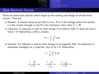
  • 2. Device Physics The Diode The Transistor Signals Basic Circuits Basic Devices Energy Bands Charge Carriers Extrinsic Semiconductors Energy Levels Basic Electronic Devices There are three basic devices which shape up the working and design of all electronic circuits. They are: Resistor- A resistor works as per Ohms Law. If V is the voltage across the resistor, I is the current through it and R is the resistance value, then V = IR. Capacitor- A capacitor is used to store energy in its electric field. It does not have a linear I-V relationship, unlike a resistor. V = 1 C Z I.dt Inductor- An inductor is used to store energy in its magnetic field. Its behaviour is somewhat analogous to a capacitor, due to its I-V relationship. I = 1 L Z V .dt + - V R I I C + - V I + - V L Debapratim Ghosh An Introduction to Basic Electronics 2/25
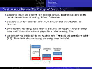
  • 3. Device Physics The Diode The Transistor Signals Basic Circuits Basic Devices Energy Bands Charge Carriers Extrinsic Semiconductors Energy Levels Semiconductor Devices- The Concept of Energy Bands Electronic circuits are different from electrical circuits. Electronics depend on the use of semiconductors as well e.g. Silicon, Germanium. Semiconductors have electrical conductivity between that of conductors and insulators. Every element has energy levels which its electrons can occupy. A range of energy levels which cause some common properties is called an energy band. We consider two energy bands- the valence band (VB) and the conduction band (CB). The valence electrons occupy the energy levels in the VB. Debapratim Ghosh An Introduction to Basic Electronics 3/25
  • 4. Device Physics The Diode The Transistor Signals Basic Circuits Basic Devices Energy Bands Charge Carriers Extrinsic Semiconductors Energy Levels The Concept of Energy Bands (contd...) What does this imply? From the band structure figure, it is clear that even at room temperature, metals have free electrons in the conduction band, which make them good conductors. The difference between the lowest energy level in the CB and the highest energy level in the VB is called a band-gap. Larger the band-gap, lesser is the conductivity. Semiconductors are insulators at room temperature. However, with an externally applied voltage, the valence electrons in the semiconductor may overcome the band-gap and climb to the CB. The band-gap is about 1.1 eV for silicon. Debapratim Ghosh An Introduction to Basic Electronics 4/25
  • 5. Device Physics The Diode The Transistor Signals Basic Circuits Basic Devices Energy Bands Charge Carriers Extrinsic Semiconductors Energy Levels Electrons and Holes In pure silicon, the presence four valence electrons is the reason to forming a matrix of silicon atoms in a crystalline structure. This property is called catenation. All electrons form a part of the covalent bonds hence there are no free charge carriers at room temperature. However, an external electric field may cause some electrons to break the covalent bonds and flow as a mobile charge (overcoming the band-gap). An electron deficiency in the crystal is called a hole. What can be said about the concentration of free electrons and holes in a pure semiconductor? Pure semiconductors are also called intrinsic semiconductors. Debapratim Ghosh An Introduction to Basic Electronics 5/25
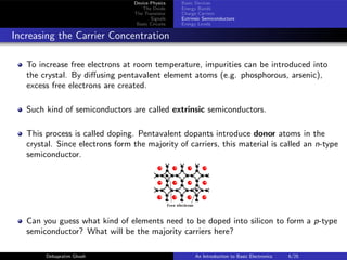
  • 6. Device Physics The Diode The Transistor Signals Basic Circuits Basic Devices Energy Bands Charge Carriers Extrinsic Semiconductors Energy Levels Increasing the Carrier Concentration To increase free electrons at room temperature, impurities can be introduced into the crystal. By diffusing pentavalent element atoms (e.g. phosphorous, arsenic), excess free electrons are created. Such kind of semiconductors are called extrinsic semiconductors. This process is called doping. Pentavalent dopants introduce donor atoms in the crystal. Since electrons form the majority of carriers, this material is called an n-type semiconductor. Can you guess what kind of elements need to be doped into silicon to form a p-type semiconductor? What will be the majority carriers here? Debapratim Ghosh An Introduction to Basic Electronics 6/25
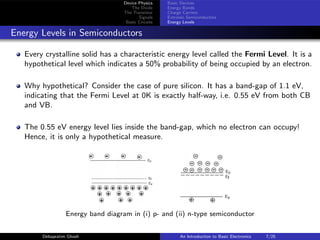
  • 7. Device Physics The Diode The Transistor Signals Basic Circuits Basic Devices Energy Bands Charge Carriers Extrinsic Semiconductors Energy Levels Energy Levels in Semiconductors Every crystalline solid has a characteristic energy level called the Fermi Level. It is a hypothetical level which indicates a 50% probability of being occupied by an electron. Why hypothetical? Consider the case of pure silicon. It has a band-gap of 1.1 eV, indicating that the Fermi Level at 0K is exactly half-way, i.e. 0.55 eV from both CB and VB. The 0.55 eV energy level lies inside the band-gap, which no electron can occupy! Hence, it is only a hypothetical measure. Energy band diagram in (i) p- and (ii) n-type semiconductor Debapratim Ghosh An Introduction to Basic Electronics 7/25
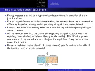
  • 8. Device Physics The Diode The Transistor Signals Basic Circuits p-n Junctions Biasing Methods The p-n Junction under Equilibrium Fusing together a p- and an n-type semiconductor results in formation of a p-n junction diode. Due to large difference in carrier concentration, the electrons from the n-side tend to diffuse to the p-side, leaving behind positively charged donor atoms behind. Likewise, the holes start moving from the p-side, leaving behind negatively charged acceptor atoms. As the electrons flow into the p-side, the negatively charged acceptor ions start repelling them (similarly with holes flowing to the n-side). This diffusion process continues until the ionized atoms at the junction repel flow of any more carriers across the junction. Hence, a depletion region (devoid of charge carriers) gets formed on either side of the junction, with a built-in potential. Debapratim Ghosh An Introduction to Basic Electronics 8/25
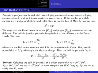
  • 9. Device Physics The Diode The Transistor Signals Basic Circuits p-n Junctions Biasing Methods The Built-in Potential Consider a p-n junction formed with donor doping concentration ND , acceptor doping concentration NA and an intrinsic carrier concentration ni . If the number of mobile carriers are n and p for electrons and holes, then as per the Law of Mass Action, we have n2 i = n.p We know that the Fermi Levels in n-type (Ef ,n) and p-type (Ef ,p) semiconductors are different. The built-in junction potential is equivalent to the difference in the Fermi Levels. We have, Ef ,n = kT ln( ND ni ) Ef ,p = kT ln( ni NA ) where k is the Boltzmann constant and T is the temperature in Kelvin. But, electric potential = E/q, where q is the electron charge. Then the built-in potential V粒 is V粒 = Ef ,n Ef ,p q = kT q ln( NAND n2 i ) Exercise: Calculate the built-in potential of a silicon diode with ni = 1010 /cm3 , ND = 1016 /cm3 and NA = 1015 /cm3 at room temperature 27 C. Vary ni , ND and NA to study how V粒 varies. Debapratim Ghosh An Introduction to Basic Electronics 9/25
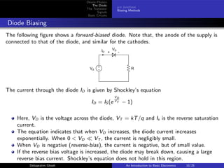
  • 10. Device Physics The Diode The Transistor Signals Basic Circuits p-n Junctions Biasing Methods Diode Biasing The following figure shows a forward-biased diode. Note that, the anode of the supply is connected to that of the diode, and similar for the cathodes. + R + - VD ID VS The current through the diode ID is given by Shockleys equation ID = IS (e VD VT 1) Here, VD is the voltage across the diode, VT = kT/q and Is is the reverse saturation current. The equation indicates that when VD increases, the diode current increases exponentially. When 0 < VD VT , the current is negligibly small. When VD is negative (reverse-bias), the current is negative, but of small value. If the reverse bias voltage is increased, the diode may break down, causing a large reverse bias current. Shockleys equation does not hold in this region. Debapratim Ghosh An Introduction to Basic Electronics 10/25
  • 11. Device Physics The Diode The Transistor Signals Basic Circuits p-n Junctions Biasing Methods What happens during forward bias? The majority carriers (holes in p-type and electrons in n-type) are pushed towards the junction due to the externally applied voltage. At the p-n junction, there are two opposing electric fields acting. One is the built-in field across the junction and the other is the influence of the externally applied voltage. The result is that the net field is less than the equilibrium field value, hence the electrons from the n-side move to the p-side, resulting in a forward-bias current. The conventional current direction is always opposite to that of the flow of electrons, hence the forward current is from the anode (p) to the cathode (n). As evident from Shockleys equation, the current increases with increase in VD . This is assuming that VD < V粒. Since the electric field in the diode is strongest at the junction, nearly all of the applied voltage is seen at the junction itself. Exercise: Work out what happens during reverse bias. Why is the current low? Why does breakdown occur? Debapratim Ghosh An Introduction to Basic Electronics 11/25
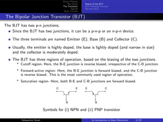
  • 12. Device Physics The Diode The Transistor Signals Basic Circuits Basics of the BJT BJT Working Principle Revision Quiz The Bipolar Junction Transistor (BJT) The BJT has two p-n junctions. Since the BJT has two junctions, it can be a p-n-p or an n-p-n device. The three terminals are named Emitter (E), Base (B) and Collector (C). Usually, the emitter is highly doped, the base is lightly doped (and narrow in size) and the collector is moderately doped. The BJT has three regions of operation, based on the biasing of the two junctions. * Cutoff region- Here, the B-E junction is reverse biased, irrespective of the C-B junction. * Forward-active region- Here, the B-E junction is forward biased, and the C-B junction is reverse biased. This is the most commonly used region of operation. * Saturation region- Here, both B-E and C-B junctions are forward biased. C E E C B B Symbols for (i) NPN and (ii) PNP transistor Debapratim Ghosh An Introduction to Basic Electronics 12/25
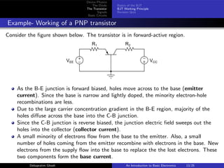
  • 13. Device Physics The Diode The Transistor Signals Basic Circuits Basics of the BJT BJT Working Principle Revision Quiz Example- Working of a PNP transistor Consider the figure shown below. The transistor is in forward-active region. + + R1 R2 VEE VCC As the B-E junction is forward biased, holes move across to the base (emitter current). Since the base is narrow and lightly doped, the minority electron-hole recombinations are less. Due to the large carrier concentration gradient in the B-E region, majority of the holes diffuse across the base into the C-B junction. Since the C-B junction is reverse biased, the junction electric field sweeps out the holes into the collector (collector current). A small minority of electrons flow from the base to the emitter. Also, a small number of holes coming from the emitter recombine with electrons in the base. New electrons from the supply flow into the base to replace the the lost electrons. These two components form the base current. Debapratim Ghosh An Introduction to Basic Electronics 13/25
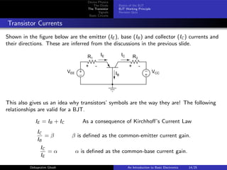
  • 14. Device Physics The Diode The Transistor Signals Basic Circuits Basics of the BJT BJT Working Principle Revision Quiz Transistor Currents Shown in the figure below are the emitter (IE ), base (IB ) and collector (IC ) currents and their directions. These are inferred from the discussions in the previous slide. + + + - + - VEE VCC R1 R2 IE IB IC This also gives us an idea why transistors symbols are the way they are! The following relationships are valid for a BJT. IE = IB + IC As a consequence of Kirchhoffs Current Law IC IB = 硫 硫 is defined as the common-emitter current gain. IC IE = 留 留 is defined as the common-base current gain. Debapratim Ghosh An Introduction to Basic Electronics 14/25
  • 15. Device Physics The Diode The Transistor Signals Basic Circuits Basics of the BJT BJT Working Principle Revision Quiz A Quick Quiz- and an Exercise! Based on what weve learnt so far, try to answer these questions. 1. What are the possible values 留 can take? 2. Would we like 硫 to be large or small? Why? 3. Mentally, try to find out a relation between 留 and 硫. 4. Suggest some applications of diodes. Exercise 1: Similar to the way we worked out for a PNP transistor, familiarize yourself with the working of an NPN transistor. Exercise 2: Find out what happens in the saturation region. Do the above current relations still hold? Debapratim Ghosh An Introduction to Basic Electronics 15/25
  • 16. Device Physics The Diode The Transistor Signals Basic Circuits Definitions and Properties Frequency Components Introduction to Signals A signal is a time-dependent piece of information. It is something that removes uncertainty in some manner. In electronics we use two kinds of signals- voltage and current. We will mostly be working with voltages. Let us look at some properties of signals. Periodicity- If x(t) is a signal and x(t + T) = x(t) t, then x(t) is said to be periodic with period T. Continuity- If a signal has a defined value at all points in time, it is a continuous-time (CT) signal. Else, it is a discrete-time (DT) signal. There are several other signal properties- determinism, causality, energy/power properties. Debapratim Ghosh An Introduction to Basic Electronics 16/25
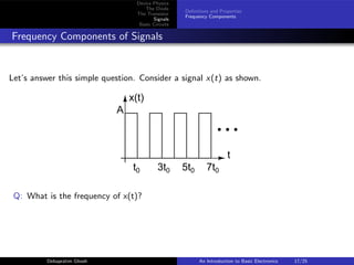
  • 17. Device Physics The Diode The Transistor Signals Basic Circuits Definitions and Properties Frequency Components Frequency Components of Signals Lets answer this simple question. Consider a signal x(t) as shown. t x(t) A t0 3t0 5t0 7t0 Q: What is the frequency of x(t)? Debapratim Ghosh An Introduction to Basic Electronics 17/25
  • 18. Device Physics The Diode The Transistor Signals Basic Circuits Definitions and Properties Frequency Components Frequency Components of Signals Lets answer this simple question. Consider a signal x(t) as shown. t x(t) A t0 3t0 5t0 7t0 Q: What is the frequency of x(t)? A: Looks simple- 1/2t0, isnt it? But not entirely! Let us see why. Debapratim Ghosh An Introduction to Basic Electronics 17/25
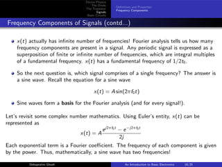
  • 19. Device Physics The Diode The Transistor Signals Basic Circuits Definitions and Properties Frequency Components Frequency Components of Signals (contd...) x(t) actually has infinite number of frequencies! Fourier analysis tells us how many frequency components are present in a signal. Any periodic signal is expressed as a superposition of finite or infinite number of frequencies, which are integral multiples of a fundamental frequency. x(t) has a fundamental frequency of 1/2t0. So the next question is, which signal comprises of a single frequency? The answer is a sine wave. Recall the equation for a sine wave x(t) = A sin(2f0t) Sine waves form a basis for the Fourier analysis (and for every signal!). Lets revisit some complex number mathematics. Using Eulers entity, x(t) can be represented as x(t) = A ej2f0t ej2f0t 2j Each exponential term is a Fourier coefficient. The frequency of each component is given by the power. Thus, mathematically, a sine wave has two frequencies! Debapratim Ghosh An Introduction to Basic Electronics 18/25
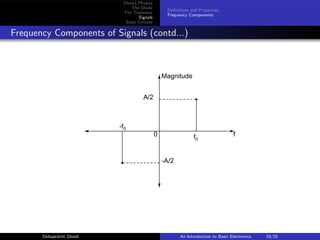
  • 20. Device Physics The Diode The Transistor Signals Basic Circuits Definitions and Properties Frequency Components Frequency Components of Signals (contd...) Magnitude f 0 f0 -f0 A/2 -A/2 Debapratim Ghosh An Introduction to Basic Electronics 19/25
  • 21. Device Physics The Diode The Transistor Signals Basic Circuits Basic Filters Revision Quiz Topics for Self Study Introduction to Basic Filters Based on what we have learnt about signals and basic electronic devices, we will now study filters. A filter is a frequency-selective circuit. This means the filter will behave differently at different frequencies. One which passes low frequencies but rejects high frequencies is called a low-pass filter. Now you know what a high-pass filter is! One which rejects high and low frequencies but passes only a certain range of frequencies is called a band-pass filter. Now you know what a band-stop filter is! Consider the case of a low-pass filter. How low frequencies will it pass, and how high frequencies will it reject? The answer is through a parameter called the cut-off frequency. Let us see a simple example. Debapratim Ghosh An Introduction to Basic Electronics 20/25
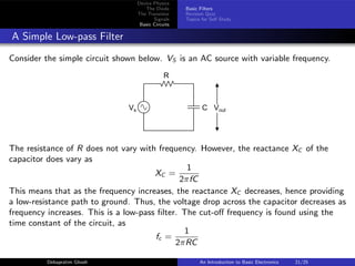
  • 22. Device Physics The Diode The Transistor Signals Basic Circuits Basic Filters Revision Quiz Topics for Self Study A Simple Low-pass Filter Consider the simple circuit shown below. VS is an AC source with variable frequency. R C Vs Vout The resistance of R does not vary with frequency. However, the reactance XC of the capacitor does vary as XC = 1 2fC This means that as the frequency increases, the reactance XC decreases, hence providing a low-resistance path to ground. Thus, the voltage drop across the capacitor decreases as frequency increases. This is a low-pass filter. The cut-off frequency is found using the time constant of the circuit, as fc = 1 2RC Debapratim Ghosh An Introduction to Basic Electronics 21/25
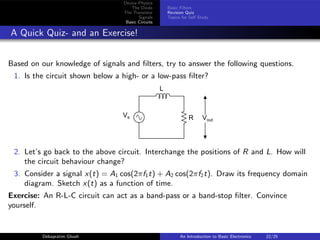
  • 23. Device Physics The Diode The Transistor Signals Basic Circuits Basic Filters Revision Quiz Topics for Self Study A Quick Quiz- and an Exercise! Based on our knowledge of signals and filters, try to answer the following questions. 1. Is the circuit shown below a high- or a low-pass filter? L R Vout Vs 2. Lets go back to the above circuit. Interchange the positions of R and L. How will the circuit behaviour change? 3. Consider a signal x(t) = A1 cos(2f1t) + A2 cos(2f2t). Draw its frequency domain diagram. Sketch x(t) as a function of time. Exercise: An R-L-C circuit can act as a band-pass or a band-stop filter. Convince yourself. Debapratim Ghosh An Introduction to Basic Electronics 22/25
  • 24. Device Physics The Diode The Transistor Signals Basic Circuits Basic Filters Revision Quiz Topics for Self Study Things You Should Know There are some useful theorems you should be familiar of, before venturing into complex electronic circuits. Kirchhoffs Current Law (KCL) and Kirchhoffs Voltage Law (KVL) Superposition Principle Thevenins and Nortons Theorem In addition, you should know certain tools and techniques to handle complex electronic circuits to make them simple. Star-Delta transforms Source transformation And many more........ Debapratim Ghosh An Introduction to Basic Electronics 23/25
  • 25. Device Physics The Diode The Transistor Signals Basic Circuits Basic Filters Revision Quiz Topics for Self Study Some Good References For circuit/network theorems Engineering Circuit Analysis by William Hayt, McGraw Hill Several good online resources For electronic devices (not just diode and BJT!) Electronic Circuit Analysis and Design by Donald A. Neamen, Tata McGraw Hill Microelectronic Circuits by Sedra and Smith, Oxford For electronics as a general overview, The Art of Electronics by Horowitz and Hill is a good read. Debapratim Ghosh An Introduction to Basic Electronics 24/25
  • 26. Device Physics The Diode The Transistor Signals Basic Circuits Basic Filters Revision Quiz Topics for Self Study References http://chemwiki.ucdavis.edu/ http://electronics-for-beginners.com http://cnx.org http://www.electronics-tutorials.ws/diode/ Donald A. Neamen, Electronic Circuits Analysis and Design, Third Edition, Tata McGraw Hill Debapratim Ghosh An Introduction to Basic Electronics 25/25