boolean algrebra and logic gates in short
ŌĆóDownload as PPT, PDFŌĆó
3 likesŌĆó1,623 views

The document discusses logic gates and Boolean algebra. It describes the basic logic gates - OR, AND, NOT, NAND, NOR and XOR gates. It explains their symbols, truth tables and functions. Logic gates are electronic circuits that make logic decisions. Boolean algebra uses values of 0 and 1 instead of numbers. It has laws like commutative, associative and distributive laws that define operations on logic values. Logic gates and Boolean algebra are important for designing digital circuits and simplifying logical functions.


boolean algrebra and logic gates in short
- 2. ŌŚ” Logic gates ŌŚ” Boolean algebra
- 3. INTRODUCTION: ’āś A logic gate is an electronic circuit/device which makes logic decisions. ’āś Most logic gates are two inputs and one outputs. ’āś At any given moment, every terminal is in one of the two binary conditions low (0) or high(1), represented by different voltage levels.
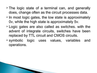
- 4. ’āś The logic state of a terminal can, and generally does, change often as the circuit processes data. ’āś In most logic gates, the low state is approximately 0v, while the high state is approximately 5v. ’āś Logic gates are also called as switches. with the advent of integrate circuits, switches have been replaced by TTL circuit and CMOS circuits. ’āś symbolic logic uses values, variables and operations.
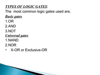
- 5. TYPES OF LOGIC GATES: The most common logic gates used are, Basic gates 1.OR 2.AND 3.NOT Universal gates 1.NAND 2.NOR ’āś X-OR or Exclusive-OR
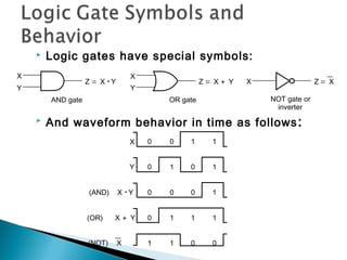
- 6. ’üĮ Logic gates have special symbols: OR gate X Y Z = X + Y ’üĮ And waveform behavior in time as follows: X 0 0 1 1 Y 0 1 0 1 (AND) X ┬Ę Y 0 0 0 1 (OR) X + Y 0 1 1 1 (NOT) X 1 1 0 0 X Y Z = X ┬Ę Y AND gate X Z = X NOT gate or inverter
- 7. OR GATE: ’āś The OR gate has two or more inputs and one output. ’āś Its output is true if at least one input is true. SYMBOL:
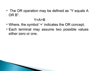
- 8. ’āś The OR operation may be defined as ŌĆ£Y equals A OR BŌĆØ. Y=A+B ’āśWhere, the symbol ŌĆś+ŌĆÖ indicates the OR concept. ’āś Each terminal may assume two possible values either zero or one.
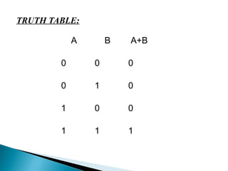
- 9. TRUTH TABLE: A B A+B 0 0 0 0 1 1 1 0 1 1 1 1
- 10. AND GATE: ’āś The AND gate is also a basic kind of digital circuit. ’āś It has also two or more inputs and one output. SYMBOL:
- 11. ’āś The AND operation for the output is defined as, ŌĆ£y equals A AND BŌĆØ. Y=A.B ’āś Where ŌĆś.ŌĆÖ symbol indicates AND operation. ’āś The output of the AND gate is one only when both inputs are one.
- 12. TRUTH TABLE: A B A+B 0 0 0 0 1 0 1 0 0 1 1 1
- 13. NOT GATE or Inverter Gate: ’āś A NOT gate is a basic gate that has one input and one output. SYMBOL:
- 14. ’āś The NOT circuit serves to invert the polarity of any input pulse apply to it. ’āś If A is the input then output ŌĆ£Y equals to NOT A or ─Ć. Y= ─Ć ’āśWhere, the bar symbol over A represents NOT or compliment operation
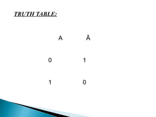
- 15. TRUTH TABLE: A ─Ć 0 1 1 0
- 16. NAND GATE: ’āś The NAND gate is known as an universal gate because it can be used to realize all the three basic functions of OR, AND & NOT gates. ’āś It is also called as NOT-AND gate. SYMBOL:
- 17. ’üĮ The Boolean expression for the NAND operation is given by, Y=A.B
- 18. TRUTH TABLE: A B AB 0 0 1 0 1 1 1 0 1 1 1 0
- 19. NOR GATE: ’āś The NOR gate is also a universal gate and it is a combination of a NOT and OR gates. SYMBOL:
- 20. ’āś The Boolean expression for NOR gate is given by, Y=A+B
- 21. TRUTH TABLE: A B A+B 0 0 1 0 1 0 1 0 0 1 1 0
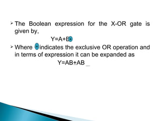
- 22. Exclusive OR or X-OR GATE: ’āś The X-OR gate is a logic gate having two inputs with and single output. SYMBOL:
- 23. ’āś The Boolean expression for the X-OR gate is given by, Y=A+B ’āśWhere + indicates the exclusive OR operation and in terms of expression it can be expanded as Y=AB+AB + +
- 24. TRUTH TABLE: A B AB+AB 0 0 0 0 1 1 1 0 1 1 1 0
- 25. ADVANTAGES OF LOGIC GATES: ’āś It is generally very easy to reliably distinguish between logic 1 or logic 0. ’āś The simplest flip-flop is the RS which is made up of two gates. ’āś K-map is also designed by using logic gates. That simplification helps when you start to connect gates to implement the functions. ’āś These gates are also used in TTL and CMOS circuitary.
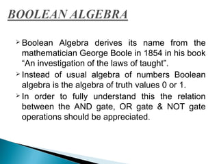
- 26. ’āś Boolean Algebra derives its name from the mathematician George Boole in 1854 in his book ŌĆ£An investigation of the laws of taughtŌĆØ. ’āś Instead of usual algebra of numbers Boolean algebra is the algebra of truth values 0 or 1. ’āś In order to fully understand this the relation between the AND gate, OR gate & NOT gate operations should be appreciated.
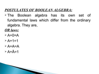
- 27. POSTULATES OF BOOLEAN ALGEBRA: ’āś The Boolean algebra has its own set of fundamental laws which differ from the ordinary algebra. They are, OR laws: ’āś A+0=A ’āś A+1=1 ’āś A+A=A ’āś A+─Ć=1
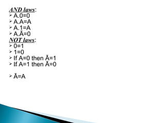
- 28. AND laws: ’āś A.0=0 ’āś A.A=A ’āś A.1=A ’āś A.─Ć=0 NOT laws: ’āś 0=1 ’āś 1=0 ’āś If A=0 then ─Ć=1 ’āś If A=1 then ─Ć=0 ’āś ─Ć=A
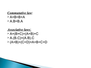
- 29. Commutative law: ’āś A+B=B+A ’āś A.B=B.A Associative laws: ’āś A+(B+C)=(A+B)+C ’āś A.(B.C)=(A.B).C ’āś (A+B)+(C+D)=A+B+C+D
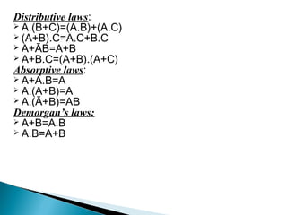
- 30. Distributive laws: ’āś A.(B+C)=(A.B)+(A.C) ’āś (A+B).C=A.C+B.C ’āś A+─ĆB=A+B ’āś A+B.C=(A+B).(A+C) Absorptive laws: ’āś A+A.B=A ’āś A.(A+B)=A ’āś A.(─Ć+B)=AB DemorganŌĆÖs laws: ’āś A+B=A.B ’āś A.B=A+B
- 31. EXAMPLE: (AB+C)(AB+D)=AB+CD ’āś AB.AB+AB.D+C.AB+C.D ’āś AB+ABD+ABC+CD {A.A=A} ’āś AB(1+D)+ABC+CD {1+A=1} ’āś AB+ABC+CD ’āś AB(1+C)+CD ’āś AB+CD
- 32. Advantages: ’āś If we use Boolean algebra for your logical problem you can save more gates and operations. so your design will be cheaper, more comprehensible, more serviceable . ’āś It allows logical steps quickly and repeatedly. Disadvantages: ’āś Can only arrive at direct results not implied once.