

chaptefffffffdddddzsjjjhhgggggggggr 2.ppt
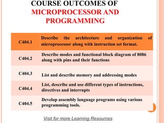
- 1. COURSE OUTCOMES OF MICROPROCESSOR AND PROGRAMMING C404.1 Describe the architecture and organization of microprocessor along with instruction set format. C404.2 Describe modes and functional block diagram of 8086 along with pins and their functions C404.3 List and describe memory and addressing modes C404.4 List, describe and use different types of instructions, directives and interrupts C404.5 Develop assembly language programs using various programming tools. Visit for more Learning Resources
- 2. ? C404.1 ? Describe the architecture and organization of microprocessor along with instruction set format. ? C404.2 ? Describe modes and functional block diagram of 8086 along with pins and their functions ? C404.3 ? List and describe memory and addressing modes ? C404.4 ? List, describe and use different types of instructions, directives and interrupts ? C404.5 ? Develop assembly language programs using various programming tools.
- 3. CHAPTER 2 16 BIT MICROPROCESSOR 8086
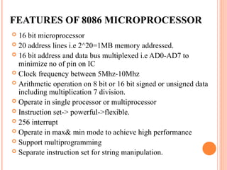
- 4. FEATURES OF 8086 MICROPROCESSOR ? 16 bit microprocessor ? 20 address lines i.e 2^20=1MB memory addressed. ? 16 bit address and data bus multiplexed i.e AD0-AD7 to minimize no of pin on IC ? Clock frequency between 5Mhz-10Mhz ? Arithmetic operation on 8 bit or 16 bit signed or unsigned data including multiplication 7 division. ? Operate in single processor or multiprocessor ? Instruction set-> powerful->flexible. ? 256 interrupt ? Operate in max& min mode to achieve high performance ? Support multiprogramming ? Separate instruction set for string manipulation.
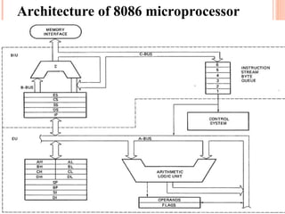
- 5. Architecture of 8086 microprocessor
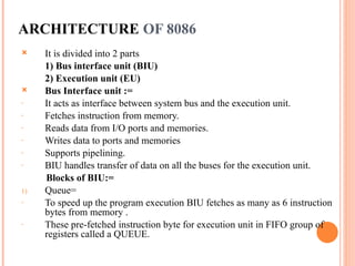
- 6. ARCHITECTURE OF 8086 ? It is divided into 2 parts 1) Bus interface unit (BIU) 2) Execution unit (EU) ? Bus Interface unit := - It acts as interface between system bus and the execution unit. - Fetches instruction from memory. - Reads data from I/O ports and memories. - Writes data to ports and memories - Supports pipelining. - BIU handles transfer of data on all the buses for the execution unit. Blocks of BIU:= 1) Queue= - To speed up the program execution BIU fetches as many as 6 instruction bytes from memory . - These pre-fetched instruction byte for execution unit in FIFO group of registers called a QUEUE.
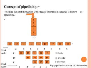
- 7. Concept of pipelining:= -fetching the next instruction while recent instruction executes is known as pipelining. - 6 5 4 3 2 1 I1 I2 I3 I4 I5 I6 I7 I8 I9 1 2 3 4 5 6 7 8 9 Clock cycle I1 I2 I3 I4 I5 I1 I2 I3 I4 I1 I2 I3 F D E F-Fetch D-Decode E-Executes 1 2 3 4 5 Clock cycle Fig: pipelined execution of 3 instruction
- 8. 1. On non pipelined processor 9 clock cycle are required for individual fetch , decode & execute for 3 instruction. 2. On pipelined processor fetch, decode & execute operation are performed in parallel. 3. -only 5 cycle are required to execute 3 instruction. 4. - 1 instruction requires -> 3 cycle to completes. 5. Additional instruction complete at rate of one per cycle. 6. During clock cycle 5 I3 instruction executing , I4 is decoding , I5 instruction fetched. 7. If 1000 instruction it requires 3000 clock cycle on non pipelined processor.----> require 1002 clock cycle on pipelined processor. 8. In 8086 performs fetch , decode , & executes instruction in parallel.
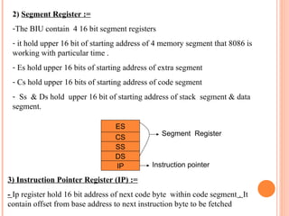
- 9. 2) Segment Register := -The BIU contain 4 16 bit segment registers - it hold upper 16 bit of starting address of 4 memory segment that 8086 is working with particular time . - Es hold upper 16 bits of starting address of extra segment - Cs hold upper 16 bits of starting address of code segment - Ss & Ds hold upper 16 bit of starting address of stack segment & data segment. ES CS SS DS IP Instruction pointer Segment Register 3) Instruction Pointer Register (IP) := - Ip register hold 16 bit address of next code byte within code segment . It contain offset from base address to next instruction byte to be fetched
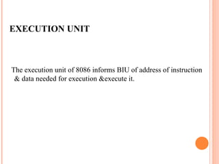
- 10. EXECUTION UNIT The execution unit of 8086 informs BIU of address of instruction & data needed for execution &execute it.
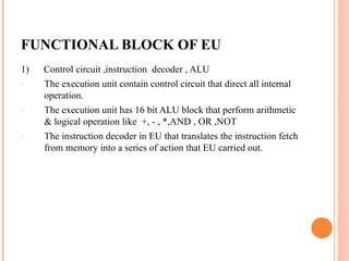
- 11. FUNCTIONAL BLOCK OF EU 1) Control circuit ,instruction decoder , ALU - The execution unit contain control circuit that direct all internal operation. - The execution unit has 16 bit ALU block that perform arithmetic & logical operation like +, - , *,AND , OR ,NOT - The instruction decoder in EU that translates the instruction fetch from memory into a series of action that EU carried out.
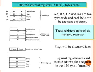
- 12. 8086/88 internal registers 16 bits (2 bytes each) AX, BX, CX and DX are two bytes wide and each byte can be accessed separately These registers are used as memory pointers. Flags will be discussed later Segment registers are used as base address for a segment in the 1 M byte of memory
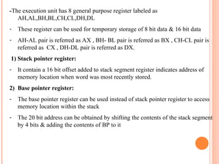
- 13. -The execution unit has 8 general purpose register labeled as AH,AL,BH,BL,CH,CL,DH,DL - These register can be used for temporary storage of 8 bit data & 16 bit data - AH-AL pair is referred as AX , BH- BL pair is referred as BX , CH-CL pair is referred as CX , DH-DL pair is referred as DX. 1) Stack pointer register: - It contain a 16 bit offset added to stack segment register indicates address of memory location when word was most recently stored. 2) Base pointer register: - The base pointer register can be used instead of stack pointer register to access memory location within the stack - The 20 bit address can be obtained by shifting the contents of the stack segment by 4 bits & adding the contents of BP to it
- 14. 3) Source index register: -The source index register is used to load 16 bit offset of a data word in data segment . -The physical address of the data word can be obtained by shifting the contents of DS register by 4 bits & adding into SI 4) Destination index register -It is used to hold the 16 bit offset of a data word in extra segment while executing string instruction -The 20 bit physical address is calculated from DS & DI
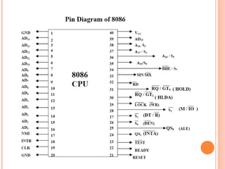
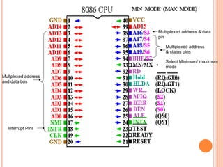
- 16. Multiplexed address & status pins Multiplexed address & data pin Select Minimum/ maximum mode Multplexed address and data bus Interrupt Pins
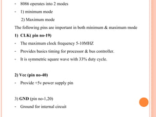
- 17. - 8086 operates into 2 modes - 1) minimum mode 2) Maximum mode The following pins are important in both minimum & maximum mode 1) CLK( pin no-19) - The maximum clock frequency 5-10MHZ - Provides basics timing for processor & bus controller. - It is symmetric square wave with 33% duty cycle. 2) Vcc (pin no-40) - Provide +5v power supply pin 3) GND (pin no-1,20) - Ground for internal circuit
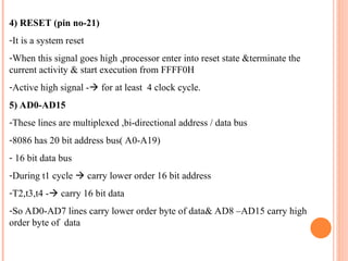
- 18. 4) RESET (pin no-21) -It is a system reset -When this signal goes high ,processor enter into reset state &terminate the current activity & start execution from FFFF0H -Active high signal -? for at least 4 clock cycle. 5) AD0-AD15 -These lines are multiplexed ,bi-directional address / data bus -8086 has 20 bit address bus( A0-A19) - 16 bit data bus -During t1 cycle ? carry lower order 16 bit address -T2,t3,t4 -? carry 16 bit data -So AD0-AD7 lines carry lower order byte of data& AD8 ©CAD15 carry high order byte of data
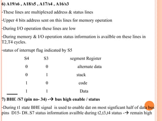
- 19. 6) A19/s6 , A18/s5 , A17/s4 , A16/s3 -These lines are multiplexed address & status lines -Upper 4 bits address sent on this lines for memory operation -During I/O operation these lines are low -During memory & I/O operation status information is availble on these lines in T2,T4 cycles. -status of interrupt flag indicated by S5 S4 S3 segment Register 0 0 alternate data 0 1 stack 1 0 code 1 1 Data 7) BHE /S7 (pin no- 34) -? bus high enable / status -During t1 state BHE signal is used to enable dat on most signficant half of data bus pins D15- D8..S7 status information availble during t2,t3,t4 status -? remain high
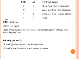
- 20. BHE A0 word /byte access 0 0 whole word from even address 0 1 upper byte from / to odd address 1 0 lower byte from / to even address 1 1 none 8) RD (pin no-32) -Active low signal -Read strobe indicates that processor is performed memory, I/O read cycle depending on s2 pin 9) Ready (pin no-22) -When high--? carry out it normal operation -When low -? freezes itĪ»s bus & enters a wait state -
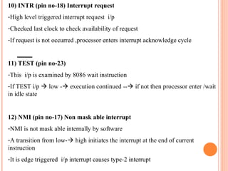
- 21. 10) INTR (pin no-18) Interrupt request -High level triggered interrupt request i/p -Checked last clock to check availability of request -If request is not occurred ,processor enters interrupt acknowledge cycle 11) TEST (pin no-23) -This i/p is examined by 8086 wait instruction -If TEST i/p ? low -? execution continued --? if not then processor enter /wait in idle state 12) NMI (pin no-17) Non mask able interrupt -NMI is not mask able internally by software -A transition from low-? high initiates the interrupt at the end of current instruction -It is edge triggered i/p interrupt causes type-2 interrupt
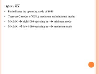
- 22. 13)MN / MX - Pin indicates the operating mode of 8086 - There are 2 modes of OS i.e maximum and minimum modes - MN/MX -? high 8086 operating in --? minimum mode - MN/MX -? low 8086 operating in --? maximum mode
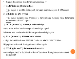
- 23. ? Signal description pins for minimum mode := 1) M/IO (pin no-28) status line:- - This signal is used to distinguish between memory access & I/O access 2) WR (pin no-29) Write:- - This signal indicates that processor is performing a memory write depending on the state of M/IO signal 3) INTA (pin no-24) interrupt acknowledge -used as an active low interrupt acknowledge signal It is used as a read strobe for interrupt acknowledge cycle 4) ALE (pin no-25) address latch enable - High ? 8086 indicates ADDR1 DATA & ADDR/STATUS bus High pulse active -? during t1 state of bus cycle 5) DT /R (pin no-27) data transmit/receive -these signal used to decide direction of data flow through the transceivers 8286/8287
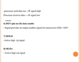
- 24. -processor send data out --? signal high Processor receives data ---? signal low 6) DEN (pin no-26) data enable - Signal provides an output enables signal for transceivers 8286 / 8287 7) HOLD -Active high i/p signal 8) HLDA - Active high o/p signal
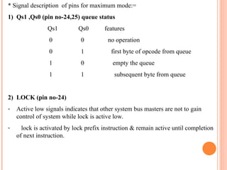
- 25. * Signal description of pins for maximum mode:= 1) Qs1 ,Qs0 (pin no-24,25) queue status Qs1 Qs0 features 0 0 no operation 0 1 first byte of opcode from queue 1 0 empty the queue 1 1 subsequent byte from queue 2) LOCK (pin no-24) - Active low signals indicates that other system bus masters are not to gain control of system while lock is active low. - lock is activated by lock prefix instruction & remain active until completion of next instruction.
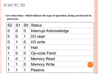
- 26. 3) S0, S1, S2 - Are status lines which indicate the type of operation, being carried out by processor. S2 S1 S0 Status 0 0 0 Interrupt Acknowledge 0 0 1 I/O read 0 1 0 I/O write 0 1 1 Halt 1 0 0 Op-code Fetch 1 0 1 Memory Read 1 1 0 Memory Write 1 1 1 Passive
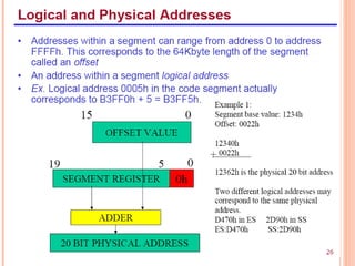
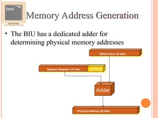
- 30. Memory Address Generation ? The BIU has a dedicated adder for determining physical memory addresses Intel Physical Address (20 Bits) Adder Segment Register (16 bits) 0 0 0 0 Offset Value (16 bits)
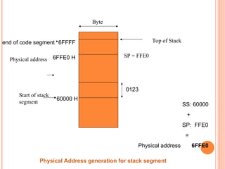
- 31. Byte 0123 60000 H 6FFE0 H 6FFFF Start of stack segment end of code segment Physical address SP = FFE0 SS: 60000 + SP: FFE0 = Physical address 6FFE0 Physical Address generation for stack segment Top of Stack
- 33. 8284 Block Diagram: Clock Logic Ready Logic Reset Logic x1 x2 EF1 RDY1 AEN1 RDY2 AEN2 RES F / C Clock OSC PCLK READY RESET CSYNC
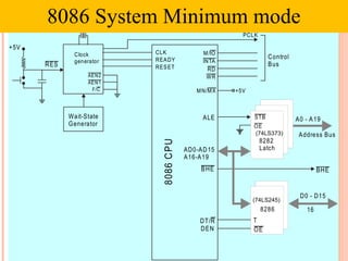
- 34. 8086 C P U F/C AEN1 AEN2 Clock generator +5V RES Wait-State Generator CLK READY RESET M/IO INTA RD WR PCLK MN/MX +5V STB OE 8282 Latch ALE AD0-AD15 A16-A19 BHE BHE D0 - D15 8286 DT/R DEN T OE 16 A0 - A19 Address Bus Control Bus 8086 System Minimum mode (74LS373) (74LS245)
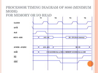
- 35. PROCESSOR TIMING DIAGRAM OF 8086 (MINIMUM MODE) FOR MEMORY OR I/O READ ALE T1 CLOCK T2 T3 T4 AD15 - AD0 A19/S6 - A16/S3 DT/R __ IO/M __ ____ RD DEN ______ A15 - A0 D0 ©C D15 (from memory) A19 - A16 S6 - S3 if I/O ACCESS this is HIGH, if MEMORY ACCESS this is LOW
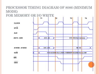
- 36. PROCESSOR TIMING DIAGRAM OF 8086 (MINIMUM MODE) FOR MEMORY OR I/O WRITE ALE T1 CLOCK T2 T3 T4 AD15 - AD0 A19/S6 - A16/S3 DT/R __ IO/M __ ____ WR DEN ______ A15 - A0 D15 - D0 (from memory) A19 - A16 S6 - S3 if I/O ACCESS this is HIGH, if MEMORY ACCESS this is LOW
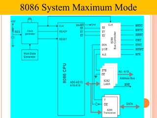
- 37. 8086 C P U Clock generator Wait-State Generator CLK READY RESET MN/MX AD0-AD15 A16-A19 BHE STB OE 8282 Latch A0 - A19 Address Bus +5V RES S0 S1 S2 CLK S0 S1 S2 DATA 8286 Transceiver T OE ALE Gnd DEN DT/R MRDC MWTC IORC IOWC AIOWC AMWC INTA 8288 B us C ontroller 8086 System Maximum Mode
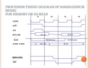
- 38. PROCESSOR TIMING DIAGRAM OF 8086(MAXIMUM MODE) FOR MEMORY OR I/O READ ALE T1 CLOCK T2 T3 T4 AD15- AD0 A19/S6 - A16/S3 DT/R __ MDRC/IORC DEN ______ A15 - A0 S6 - S3 A19 - A16 D0-D15 S2-S0 S2-S0 Active S2-S0 Inacive
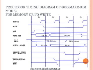
- 39. PROCESSOR TIMING DIAGRAM OF 8086(MAXIMUM MODE) FOR MEMORY OR I/O WRITE ALE T1 CLOCK T2 T3 T4 AD15- AD0 A19/S6 - A16/S3 DT/R __ AMWC/AIOWC DEN ______ A15 - A0 S6 - S3 A19 - A16 D0-D15 S2-S0 S2-S0 Active S2-S0 Inacive MWTC &IOWC For more detail contact us