
digitalvoltmeterusing805112b2-170214173216 (1).pdf
- 1. DIGITAL VOLTMETER USING 8051 MICRO CONTROLLER
- 2. CONTENT-1 ? INTRODUCTION ? DIGITAL VOLTMETER ? MICROCONTROLLER ? CIRCUIT DIAGRAM OF DIGITAL VOLMETER ? COMPONENTS REQUIRED IN THE CIRCUIT ? ADC 0804 ? SUCCESSIVE TYPE ADC ? LCD DISPLAY ? TOPICS TO BE COVERED IN NEXT REVIEW ? REFERENCES
- 3. CONTENT-2 ? ADC0804 INTERFACING ? ADC0804 PIN DESCRIPTION ? ADC0804 TIMING DIAGRAM ? PROGRAMMING OF ADC0804 IN C (KEIL) ? LCD INTERFACING ? LCD PIN DESCRIPTION ? LCD TIMING DIAGRAM ? LCD ADDRESSING ? SIMULATION IN PROTEUS
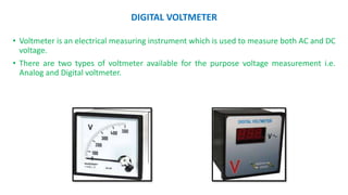
- 4. DIGITAL VOLTMETER ? Voltmeter is an electrical measuring instrument which is used to measure both AC and DC voltage. ? There are two types of voltmeter available for the purpose voltage measurement i.e. Analog and Digital voltmeter.
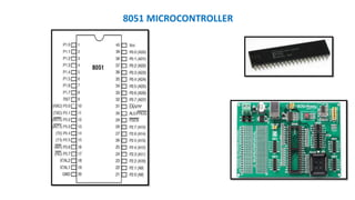
- 5. MICROCONTROLLER ? A micro controller is an integrated circuit or a chip with a processor and other support devices like program memory, data memory, I/O ports, serial communication interface etc. integrated together. ? Here Digital Voltmeter uses 8051 microcontroller. ? 8051 microcontroller is a chip having 40 pins. ? The function of 8051 microcontroller is to manipulate digital data which is obtained from analog to digital converter.
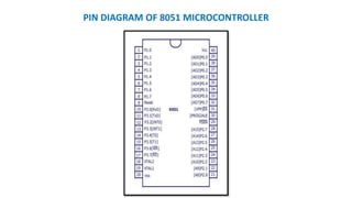
- 7. PIN DIAGRAM OF 8051 MICROCONTROLLER
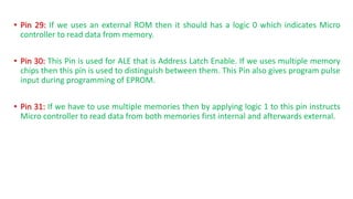
- 8. ? PIN 9: PIN 9 is the reset pin which is used to reset the microcontrollerĪ»s internal registers and ports upon starting up. (Pin should be held high for 2 machine cycles.) ? PINS 18 & 19: The 8051 has a built-in oscillator amplifier hence we need to only connect a crystal at these pins to provide clock pulses to the circuit. ? PIN 40 and 20: Pins 40 and 20 are VCC and ground respectively. The 8051 chip needs +5V 500mA to function properly, although there are lower powered versions like the Atmel 2051 which is a scaled down version of the 8051 which runs on +3V. ? PINS 29, 30 & 31: As described in the features of the 8051, this chip contains a built-in flash memory. In order to program this we need to supply a voltage of +12V at pin 31. If external memory is connected then PIN 31, also called EA/VPP, should be connected to ground to indicate the presence of external memory. PIN 30 is called ALE (address latch enable), which is used when multiple memory chips are connected to the controller and only one of them needs to be selected.We will deal with this in depth in the later chapters. PIN 29 is called PSEN. This is "program store enable". In order to use the external memory it is required to provide the low voltage (0) on both PSEN and EA pins.
- 9. ? Pin 29: If we uses an external ROM then it should has a logic 0 which indicates Micro controller to read data from memory. ? Pin 30: This Pin is used for ALE that is Address Latch Enable. If we uses multiple memory chips then this pin is used to distinguish between them. This Pin also gives program pulse input during programming of EPROM. ? Pin 31: If we have to use multiple memories then by applying logic 1 to this pin instructs Micro controller to read data from both memories first internal and afterwards external.
- 10. ? There are 4 8-bit ports: P0, P1, P2 and P3. ? PORT P1 (Pins 1 to 8): The port P1 is a general purpose input/output port which can be used for a variety of interfacing tasks. The other ports P0, P2 and P3 have dual roles or additional functions associated with them based upon the context of their usage. The port 1 output buffers can sink/source four TTL inputs. When 1s are written to portn1 pins are pulled high by the internal pull-ups and can be used as inputs. ? PORT P3 (Pins 10 to 17): PORT P3 acts as a normal IO port, but Port P3 has additional functions such as, serial transmit and receive pins, 2 external interrupt pins, 2 external counter inputs, read and write pins for memory access. ? PORT P2 (pins 21 to 28): PORT P2 can also be used as a general purpose 8 bit port when no external memory is present, but if external memory access is required then PORT P2 will act as an address bus in conjunction with PORT P0 to access external memory.
- 11. ? PORT P0 (pins 32 to 39): PORT P0 can be used as a general purpose 8 bit port when no external memory is present, but if external memory access is required then PORT P0 acts as a multiplexed address and data bus that can be used to access external memory in conjunction with PORT P2. P0 acts as AD0-AD7, as can be seen from fig 1.1 ? PIN 10: asynchronous communication input or Serial synchronous communication output. ? PIN11:Serial Asynchronous Communication Output or Serial Synchronous Communication clock Output.
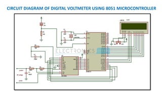
- 12. CIRCUIT DIAGRAM OF DIGITAL VOLTMETER USING 8051 MICROCONTROLLER
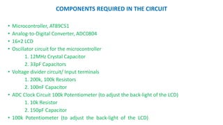
- 13. COMPONENTS REQUIRED IN THE CIRCUIT ? Microcontroller, AT89C51 ? Analog®\to®\Digital Converter, ADC0804 ? 16Ī┴2 LCD ? Oscillator circuit for the microcontroller 1. 12MHz Crystal Capacitor 2. 33pF Capacitors ? Voltage divider circuit/ Input terminals 1. 200k, 100k Resistors 2. 100nF Capacitor ? ADC Clock Circuit 100k Potentiometer (to adjust the back®\light of the LCD) 1. 10k Resistor 2. 150pF Capacitor ? 100k Potentiometer (to adjust the back®\light of the LCD)
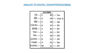
- 14. ANALOG TO DIGITAL CONVERTER(ADC0804)
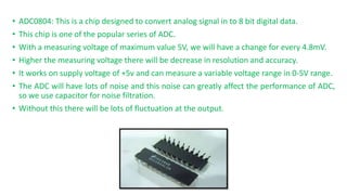
- 15. ? ADC0804: This is a chip designed to convert analog signal in to 8 bit digital data. ? This chip is one of the popular series of ADC. ? With a measuring voltage of maximum value 5V, we will have a change for every 4.8mV. ? Higher the measuring voltage there will be decrease in resolution and accuracy. ? It works on supply voltage of +5v and can measure a variable voltage range in 0-5V range. ? The ADC will have lots of noise and this noise can greatly affect the performance of ADC, so we use capacitor for noise filtration. ? Without this there will be lots of fluctuation at the output.
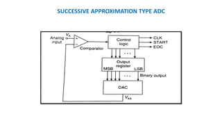
- 16. ? It is a CMOS 8 bit successive approximation type A/D converter, which translate the analog voltage at the input into a 8 bit digital word at the output. ? An increase in the analog input voltage give a corresponding increase of a single binary count of the encoder of the ADC. ? The 8 bit digital word at the output of the encoder (ADC) is loaded into one of the four ports of the microcontroller which is made of 8 data line, where they are computed and converted to the decimal equivalent and sent to the liquid crystal display (LCD) where it displays the decimal value computed by the microcontroller, which indicates the value of the analogue ac/dc voltage signal measured.
- 17. SUCCESSIVE APPROXIMATION TYPE ADC
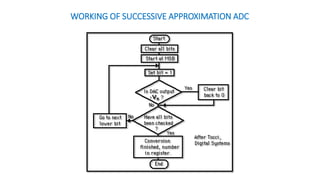
- 18. WORKING OF SUCCESSIVE APPROXIMATION ADC
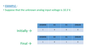
- 19. ? EXAMPLE : ? Suppose that the unknown analog input voltage is 10.3 V. (D3)MSB D2 D1 (D0)LSB 1 0 0 0 Initially Ī· (D3)MSB D2 D1 (D0)LSB 1 0 1 0 Final Ī·
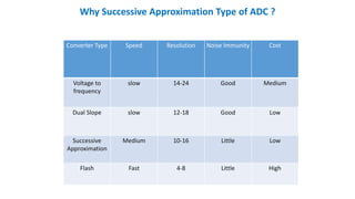
- 21. Converter Type Speed Resolution Noise Immunity Cost Voltage to frequency slow 14-24 Good Medium Dual Slope slow 12-18 Good Low Successive Approximation Medium 10-16 Little Low Flash Fast 4-8 Little High Why Successive Approximation Type of ADC ?
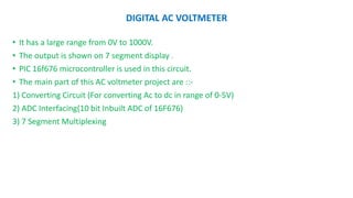
- 22. DIGITAL AC VOLTMETER ? It has a large range from 0V to 1000V. ? The output is shown on 7 segment display . ? PIC 16f676 microcontroller is used in this circuit. ? The main part of this AC voltmeter project are ::- 1) Converting Circuit (For converting Ac to dc in range of 0-5V) 2) ADC Interfacing(10 bit Inbuilt ADC of 16F676) 3) 7 Segment Multiplexing
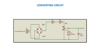
- 24. ? The bridge rectifier which is made from diodes In4007 ? It convert Ac Voltage to Dc Voltage. ? Next is Voltage divider circuit which converts any voltage from 0 to 1000v to 0 to 5v range. ? It is made using two resistors and a potential meter in series. ? Next capacitor is used for removing ripples . ? The Zener 5.1V is used for protection and it will never give voltage to controller more than 5.1 V.
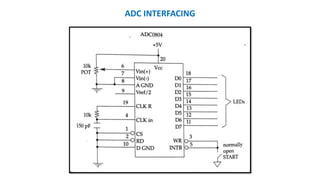
- 25. ADC INTERFACING
- 26. PIN CONFIGURATION ?CS: Chip select is Active low input used to active the ADC0804 chip.To access the ADC, this pin must be low. ?WR (start conversion): ? This is an active low input used to inform the ADC to start the conversion process. ? If CS=0 when WR makes a low-to-high transition , the ADC0804 starts converting the Analog input value of Vin to an 8-bit digital number. ? The amount of time it takes to convert varies depending on the CLK IN and CLK R values. ?CLK IN and CLK R: ? CLK IN is an input pin connected to an external clock source when an external clock is used for timing. ? ADC0804 also has an internal clock generator. To use the internal clock generator(also called self-clocking of the ADC0804), the CLK IN and CLK R pins are connected to a capacitor and a resistor as shown in above figure.
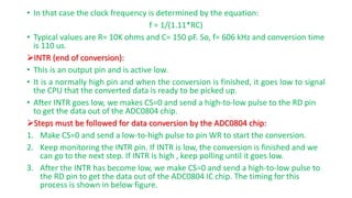
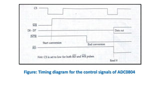
- 27. ? In that case the clock frequency is determined by the equation: f = 1/(1.11*RC) ? Typical values are R= 10K ohms and C= 150 pF. So, f= 606 kHz and conversion time is 110 us. ?INTR (end of conversion): ? This is an output pin and is active low. ? It is a normally high pin and when the conversion is finished, it goes low to signal the CPU that the converted data is ready to be picked up. ? After INTR goes low, we makes CS=0 and send a high-to-low pulse to the RD pin to get the data out of the ADC0804 chip. ?Steps must be followed for data conversion by the ADC0804 chip: 1. Make CS=0 and send a low-to-high pulse to pin WR to start the conversion. 2. Keep monitoring the INTR pin. If INTR is low, the conversion is finished and we can go to the next step. If INTR is high , keep polling until it goes low. 3. After the INTR has become low, we make CS=0 and send a high-to-low pulse to the RD pin to get the data out of the ADC0804 IC chip. The timing for this process is shown in below figure.
- 28. Figure: Timing diagram for the control signals of ADC0804
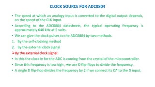
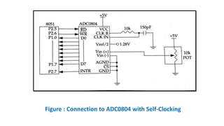
- 29. CLOCK SOURCE FOR ADC0804 ? The speed at which an analogy input is converted to the digital output depends, on the speed of the CLK input. ? According to the ADC0804 datasheets, the typical operating frequency is approximately 640 kHz at 5 volts. ? We can give the clock pulses to the ADC0804 by two methods. 1. By the self-clocking method 2. By the external clock signal ?By the external clock signal: ? In this the clock in for the ADC is coming from the crystal of the microcontroller. ? Since this frequency is too high , we use D flip-flops to divide the frequency. ? A single D flip-flop divides the frequency by 2 if we connect its Q* to the D input.
- 30. Figure : Connection to ADC0804 with Self-Clocking
- 31. Figure : 8051 Connection to ADC0804 with Clock from XTAL2 of the 8051
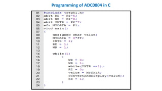
- 32. Programming of ADC0804 in C
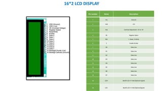
- 33. Pin number Name Description 1 Vss Ground 2 Vdd +5V 3 Vee Contrast Adjustment ®\2V to ®\5V 4 RS Register Select 5 RW 1 ®\Read , 0®\Write 6 E Enable Strobe 7 D0 Data Line 8 D1 Data Line 9 D2 Data Line 10 D3 Data Line 11 D4 Data Line 12 D5 Data Line 13 D6 Data Line 14 D7 Data Line 15 LED+ Backlit LED +V Vdd (Optional signal) 16 LED- Backlit LED +V Vdd (Optionalsignal) 16*2 LCD DISPLAY
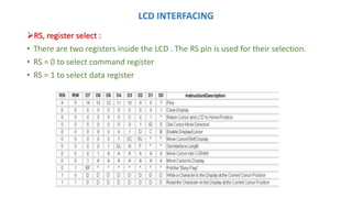
- 34. LCD INTERFACING ?RS, register select : ? There are two registers inside the LCD . The RS pin is used for their selection. ? RS = 0 to select command register ? RS = 1 to select data register
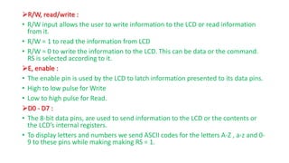
- 35. ?R/W, read/write : ? R/W input allows the user to write information to the LCD or read information from it. ? R/W = 1 to read the information from LCD ? R/W = 0 to write the information to the LCD. This can be data or the command. RS is selected according to it. ?E, enable : ? The enable pin is used by the LCD to latch information presented to its data pins. ? High to low pulse for Write ? Low to high pulse for Read. ?D0 - D7 : ? The 8-bit data pins, are used to send information to the LCD or the contents or the LCDĪ»s internal registers. ? To display letters and numbers we send ASCII codes for the letters A-Z , a-z and 0- 9 to these pins while making making RS = 1.
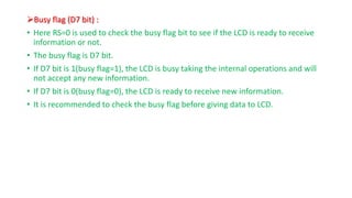
- 36. ?Busy flag (D7 bit) : ? Here RS=0 is used to check the busy flag bit to see if the LCD is ready to receive information or not. ? The busy flag is D7 bit. ? If D7 bit is 1(busy flag=1), the LCD is busy taking the internal operations and will not accept any new information. ? If D7 bit is 0(busy flag=0), the LCD is ready to receive new information. ? It is recommended to check the busy flag before giving data to LCD.
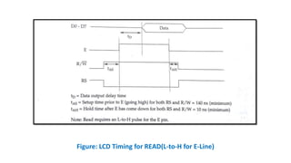
- 37. Figure: LCD Timing for READ(L-to-H for E-Line)
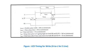
- 38. Figure : LCD Timing for Write (H-to-L for E Line)
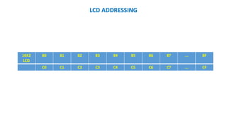
- 39. LCD ADDRESSING 16X2 LCD 80 81 82 83 84 85 86 87 ... 8F C0 C1 C2 C3 C4 C5 C6 C7 ĪŁ CF
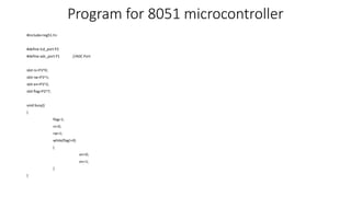
- 40. Program for 8051 microcontroller #include<reg51.h> #define lcd_port P2 #define adc_port P1 //ADC Port sbit rs=P3^0; sbit rw=P3^1; sbit en=P3^2; sbit flag=P2^7; void busy() { flag=1; rs=0; rw=1; while(flag!=0) { en=0; en=1; } }
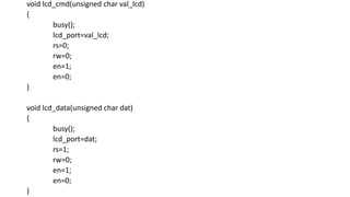
- 41. void lcd_cmd(unsigned char val_lcd) { busy(); lcd_port=val_lcd; rs=0; rw=0; en=1; en=0; } void lcd_data(unsigned char dat) { busy(); lcd_port=dat; rs=1; rw=0; en=1; en=0; }
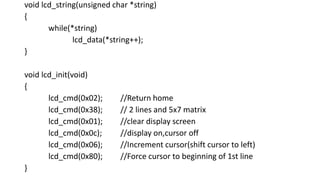
- 42. void lcd_string(unsigned char *string) { while(*string) lcd_data(*string++); } void lcd_init(void) { lcd_cmd(0x02); //Return home lcd_cmd(0x38); // 2 lines and 5x7 matrix lcd_cmd(0x01); //clear display screen lcd_cmd(0x0c); //display on,cursor off lcd_cmd(0x06); //Increment cursor(shift cursor to left) lcd_cmd(0x80); //Force cursor to beginning of 1st line }
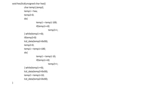
- 43. void hex2lcd(unsigned char hex){ char temp1,temp2; temp1 = hex; temp2=0; do{ temp1 = temp1-100; if(temp1>=0) temp2++; } while(temp1>=0); if(temp2>0) lcd_data(temp2+0x30); temp2=0; temp1 = temp1+100; do{ temp1 = temp1-10; if(temp1>=0) temp2++; } while(temp1>=0); lcd_data(temp2+0x30); temp2 = temp1+10; lcd_data(temp2+0x30); }
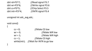
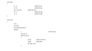
- 44. sbit rd=P3^7; //Read signal P3.7 sbit wr=P3^6; //Write signal P3.6 sbit cs=P3^5; //Chip Select P3.5 sbit intr=P3^4; //INTR signal P3.4 unsigned int adc_avg,adc; void conv() { cs = 0; //Make CS low wr = 0; //Make WR low wr = 1; //Make WR high cs = 1; //Make CS high while(intr); //Wait for INTR to go low }
- 45. void read() { cs = 0; //Make CS low rd = 0; //Make RD low adc = adc_port; //Read ADC port rd = 1; //Make RD high cs = 1; //Make CS high } void main() { char i; lcd_init(); lcd_string("Voltmeter"); while(1) { //Forever loop adc_avg = 0; for(i=0;i<10;i++) { conv(); //Start conversion read(); //Read ADC adc_avg += adc; }
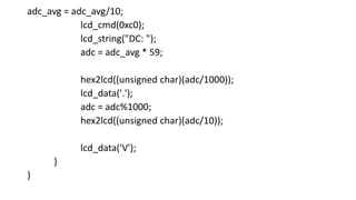
- 46. adc_avg = adc_avg/10; lcd_cmd(0xc0); lcd_string("DC: "); adc = adc_avg * 59; hex2lcd((unsigned char)(adc/1000)); lcd_data('.'); adc = adc%1000; hex2lcd((unsigned char)(adc/10)); lcd_data('V'); } }
- 47. REFERENCES ? The 8051 Microcontroller and Embedded Systems by Muhammad Ali Mazidi, Janice Gillispie Mazidi ? The 8051 Microcontroller By Ayala