DLDLab 8 half adder
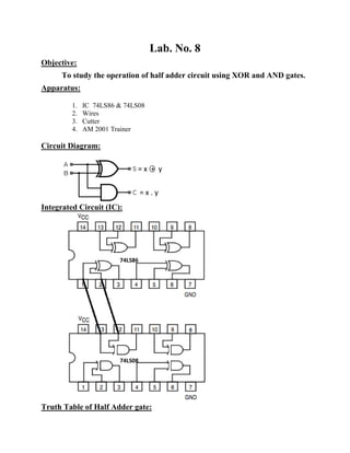
- 2. Lab. No. 8 Objective: To study the operation of half adder circuit using XOR and AND gates. Apparatus: 1. IC 74LS86 & 74LS08 2. Wires 3. Cutter 4. AM 2001 Trainer Circuit Diagram: Integrated Circuit (IC): Truth Table of Half Adder gate: 74LS86 74LS08 = x + y = x . y
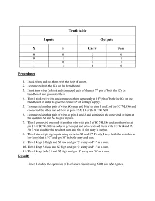
- 3. Truth table Inputs Outputs X y Carry Sum 0 0 0 0 0 1 0 1 1 0 0 1 1 1 1 0 Procedure: 1. I took wires and cut them with the help of cutter. 2. I connected both the ICs on the breadboard. 3. I took two wires (white) and connected each of them at 7th pin of both the ICs on breadboard and grounded them. 4. Then I took two wires and connected them separately at 14th pin of both the ICs on the breadboard in order to give the circuit 5V of voltage supply. 5. I connected another pair of wires (Orange and blue) at pins 1 and 2 of the IC 74LS86 and connected the other end of them at pins 12 & 13 of the IC 74LS08. 6. I connected another pair of wires at pins 1 and 2 and connected the other end of them at the switches S1 and S7 to give inputs. 7. Then I connected one end of another wire with pin 3 of IC 74LS86 and another wire at pin 11 of IC74LS08 in order to get output and other ends of them with LEDs l4 and l5. Pin 3 was used for the result of sum and pin 11 for carryĄŊs output. 8. Then I started giving inputs using switches S1 and S7. Firstly I keep both the switches at low level that is Ą°0Ąą and got Ą°0Ąą in both carry and sum. 9. Then I keep S1 high and S7 low and got ĄŪ0ĄŊ carry and ĄŪ1ĄŊ as a sum. 10. Then I keep S1 low and S7 high and got ĄŪ0ĄŊ carry and ĄŪ1ĄŊ as a sum. 11. Then I keep both S1 and S7 high and got ĄŪ1ĄŊ carry and ĄŪ0ĄŊ as a sum. Result: Hence I studied the operation of Half adder circuit using XOR and AND gates.


