ECS 2008 Presentaion
- 1. NiSi Formation in Electrochemically-Etched Silicon Nanowires W. Xu* ,1 , Vadim Palshin 2 , J.C. Flake** ,1 1 Gordon and Mary Cain Department of Chemical Engineering 2 Center for Advanced Microstructure and Devices Louisiana State University, Baton Rouge LOUISIANA STATE UNIVERSITY
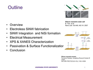
- 2. O utline Overview Electroless SiNW fabrication SiNW Integration and NiSi formation Electrical Measurement XPS & XANES Characterization Passivation & Surface Functionalization Conclusion Silicon nanowire sensor Fernando Patolsky, Gengfeng Zheng & Charles M Lieber, NATURE PROTOCOLS VOL.1 NO.4 2006 Silicon nanowire solar cell B. Tian, et al. Nano Lett. Vol.449, NO.18 2007 LOUISIANA STATE UNIVERSITY
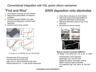
- 3. Conventional Integration with VSL grown silicon nanowires Silicon nanowire transistor (SBFETs) W. Weber. et al. Nano Lett. Vol. 6, No. 12 2006 Grow Silicon nanowire via VLS method Deposit fabricated SiNWs on dielectric substrate Find the deposited SiNWs and make electrode by lithography involved metal deposition Anneal to form ohmic contact Grow silicon nanowire via VLS method Randomly deposit fabricated SiNWs on patternted electrodes by lithography Selective electroless nickel on top of the electrode Anneal to form ohmic contact Characteristic of this approach: Find and wire time consuming High vaccum, high temperature,high costs Doping requires p-or n- type growth sequences ˇ° Find and Wireˇ± SiNW deposition onto electrodes Characteristic of this approach: Advantage over ˇ°find and wireˇ± Difficult to position nanowires, dop ing SBFET requires higher potentials VLS relatively high cost same as ˇ°find and wireˇ± C. M Lieber et al SCIENCE VOL 291 851-853 2001 . LOUISIANA STATE UNIVERSITY
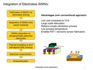
- 4. Integration of Electroless SiNWs: Fabrication of SiNWs via electroless etching SiNWs deposition on lithographically patterned electrodes Thermal annealing to form self-aligned NiSi contacts Electrical measurement Advantages over conventional approach: Low cost compared to VLS L arge scale fabrication R elative simple silicidation process Low process temperatu re Enables FET / nanowire sensor fabrication. Characterization Separation of SiNWs from parent substrate LOUISIANA STATE UNIVERSITY
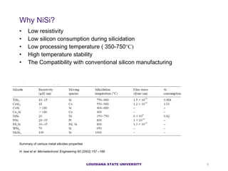
- 5. Why NiSi? Low resistivity Low silicon consumption during silicidation Low processing temperature ( 350-750 ˇăC) High temperature stability The Compatibility with conventional silicon manufacturing LOUISIANA STATE UNIVERSITY Summary of various metal silicides properties H. Iwai et al. Microelectronic Engineering 60 (2002) 157 ¨C169
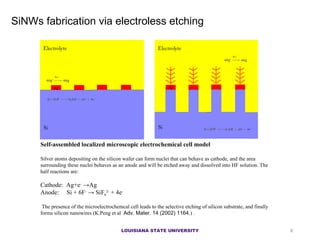
- 6. SiNW s fabrication via electroless etching Self-assembled localized microscopic electrochemical cell model Silver atoms depositing on the silicon wafer can form nuclei that can behave as cathode, and the area surrounding these nuclei behaves as an anode and will be etched away and dissolved into HF solution. The half reactions are: Cathode: Ag+e - ->Ag Anode: Si + 6F - -> SiF 6 2- + 4e - The presence of the microelectrochemcal cell leads to the selective etching of silicon substrate, and finally forms silicon nanowires (K.Peng et al Adv. Mater. 14 (2002) 1164. ) . LOUISIANA STATE UNIVERSITY
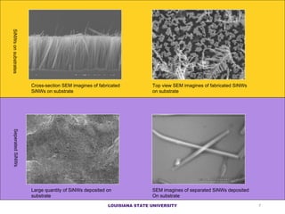
- 7. Cross-section SEM imagines of fabricated SiNWs on substrate SEM imagines of sep a rated SiNWs deposited On substrate Large quantity of SiNWs deposited on substrate To p view SEM imagines of fabricated SiNWs on substrate S iNWs on substrates Se perated SiNWs LOUISIANA STATE UNIVERSITY
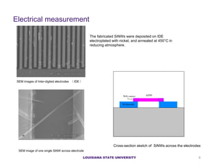
- 8. E lectrical measurement SEM images of Inter-digited electrodes Ł¨ IDE Ł© SEM image of one single SiNW across electrode The fabricated SiNWs were deposited on IDE electroplated with nickel, and annealed at 450ˇăC in reducing atmosphere. Cross-section sketch of SiNWs across the electrodes LOUISIANA STATE UNIVERSITY
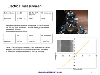
- 9. Electrical measurement Based on the estimation that there are 612 SiNWs across the IDE( by SEM analysis) ˇˇ and the average diameter of nanowire is 150 nm. ˇˇ The corresponding resistivity: Same order of magnitude of silicon for annealed nanowires suggests the lateral NiSi formation is occurred at the end of nanowires and the nanowires is not fully silicized. LOUISIANA STATE UNIVERSITY Bu lk resistance Bare IDE IDE after SiNW deposition IDE after anneal Resistance >1ˇ¤10 9 ¦¸ ˇˇŁ¨ŁĎŁĂŁ© 4ˇ¤10 6 ¦¸ 2ˇ¤10 3 ¦¸ NiSi Silicon IDE after anneal Resistivity 10¦Ě¦¸?cm 1-5 ¦¸?cm ˇ« 0.35 ¦¸?cm
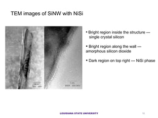
- 10. TEM images of SiNW with NiSi Bright region inside the structure --- single crystal silicon Bright region along the wall --- amorphous silicon dioxide Dark region on top right --- NiSi phase LOUISIANA STATE UNIVERSITY
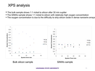
- 11. The bulk sample shows 1:1 nickel to silicon after 30 min suptter The SiNWs sample shows 1:1 nickel to silicon with relatively high oxygen concentration The oxygen concentration is due to the difficulty to strip silicon oxide in dense nanowire arrays XPS analysis Bulk silicon sample SiNWs sample LOUISIANA STATE UNIVERSITY
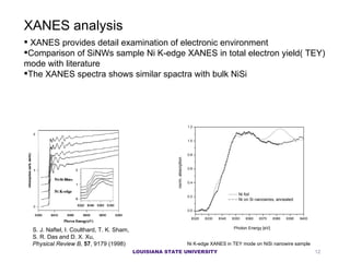
- 12. XANES provides detail examination of electronic environment Comparison of SiNWs sample Ni K-edge XANES in total electron yield( TEY) mode with literature The XANES spectra shows similar spactra with bulk NiSi XANES analysis S. J. Naftel, I. Coulthard, T. K. Sham, S. R. Das and D. X. Xu, Physical Review B , 57 , 9179 (1998) Ni K-edge XANES in TEY mode on NiSi nanowire sample LOUISIANA STATE UNIVERSITY
- 13. LOUISIANA STATE UNIVERSITY Electroless fabrication of SiNWs Separation and integration SiNWs with Patterned nickel electrodes Silicidation by thermal annealing Ohmic behavior after silicidation Problems needs to be addressed Passivation ¨C surface functionalization Doping
- 14. Directly Functionalize (Si-C, no intermediate oxide) of silicon nanowire surface as a possible solution to passivate the surface and avoid oxidation. For example anodic electrografting of SiNW surfaces with alkyl Grignards (or cathodic electrografting with alkynes) Passivation of Si surface Absorption infrared spectra. [a] ethyl hydrosilylated; [b] ethyl electrografted; [c] methyl hydrosilylated; [d] methyl electrografted. AFM images of passivated silicon surfaces. [A] ethyl anodic electrografting; [B] ethyl hydrosilylation; [C] methyl anodic electrografting; [D] methyl hydrosilylation. Anodic electrografting Thermal hydrosilylation Oxides (XPS) LOUISIANA STATE UNIVERSITY
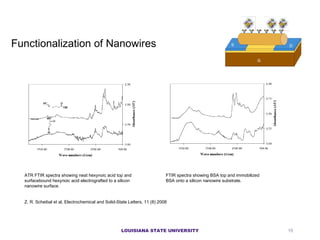
- 15. LOUISIANA STATE UNIVERSITY Functionalization of Nanowires ATR FTIR spectra showing neat hexynoic acid top and surfacebound hexynoic acid electrografted to a silicon nanowire surface. FTIR spectra showing BSA top and immobilized BSA onto a silicon nanowire substrate. Z. R. Scheibal et al, Electrochemical and Solid-State Letters, 11 (8) 2008
- 16. Conclusion Ele ctrole ss fabrication of SiNW Separation and Integration with Lithographically patterned electrode TEM, XPS, XANES Demonstrate the formation of NiSi (1:1) phase formation with pre- patternted electrodes Control surface chemistry Si-R Passivation Functionalization Current work focuses on building SiNW sensors (doping) LOUISIANA STATE UNIVERSITY
- 17. Acknowledgements: Sponsors: ATMI, Louisiana Board of Regents D. Cao Materials Characterization center, LSU S. S. Vegunta and J. N. Ngunjiri, Department of Chemical Engineering, LSU Thank you for your attention ! LOUISIANA STATE UNIVERSITY
![Directly Functionalize (Si-C, no intermediate oxide) of silicon nanowire surface as a possible solution to passivate the surface and avoid oxidation. For example anodic electrografting of SiNW surfaces with alkyl Grignards (or cathodic electrografting with alkynes) Passivation of Si surface Absorption infrared spectra. [a] ethyl hydrosilylated; [b] ethyl electrografted; [c] methyl hydrosilylated; [d] methyl electrografted. AFM images of passivated silicon surfaces. [A] ethyl anodic electrografting; [B] ethyl hydrosilylation; [C] methyl anodic electrografting; [D] methyl hydrosilylation. Anodic electrografting Thermal hydrosilylation Oxides (XPS) LOUISIANA STATE UNIVERSITY](https://image.slidesharecdn.com/ecs2008presentaion-12597254575757-phpapp01/85/ECS-2008-Presentaion-14-320.jpg)
