Electronic devices-and-circuit-theory-10th-ed-boylestad-chapter-8
ŌĆó
25 likesŌĆó7,920 views

This chapter discusses FET amplifiers. It describes the common FET configurations including common-source, common-gate, and common-drain. It provides the small-signal models and defines terms like transconductance. It then gives the input and output impedances and voltage gain calculations for each configuration. Examples of biased circuits are also presented along with a troubleshooting guide.


Electronic devices-and-circuit-theory-10th-ed-boylestad-chapter-8
- 1. Chapter 8: FET Amplifiers
- 2. Introduction FETs provide: ŌĆó Excellent voltage gain ŌĆó High input impedance ŌĆó Low-power consumption ŌĆó Good frequency range Copyright ┬®2009 by Pearson Education, Inc. Upper Saddle River, New Jersey 07458 ŌĆó All rights reserved. Electronic Devices and Circuit Theory, 10/e Robert L. Boylestad and Louis Nashelsky 2
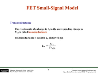
- 3. FET Small-Signal Model Transconductance The relationship of a change in ID to the corresponding change in VGS is called transconductance Transconductance is denoted gm and given by: D m I g ╬ö = GS V ╬ö Copyright ┬®2009 by Pearson Education, Inc. Upper Saddle River, New Jersey 07458 ŌĆó All rights reserved. Electronic Devices and Circuit Theory, 10/e Robert L. Boylestad and Louis Nashelsky 3
- 4. Graphical Determination of gm Copyright ┬®2009 by Pearson Education, Inc. Upper Saddle River, New Jersey 07458 ŌĆó All rights reserved. Electronic Devices and Circuit Theory, 10/e Robert L. Boylestad and Louis Nashelsky 4
- 5. Mathematical Definitions of gm D I ╬ö m V GS g ╬ö = ŌÄż ŌÄźŌÄ” ŌÄĪ DSS 2I = ŌłÆ ŌÄóŌÄŻ GS m V P P V 1 V g DSS m0 V P 2I g = ŌÄĪ ŌÄż Where VGS =0V ŌÄźŌÄ” = ŌłÆ ŌÄóŌÄŻ GS m m0 V P V g g 1 D DSS V GS 1 ŌłÆ = P I I V ŌÄø V ŌÄ× I Where D DSS m0 GS 1 g g = ŌĤŌĤŌÄĀ m m0 I P g V ŌÄ£ ŌÄ£ŌÄØ = ŌłÆ Copyright ┬®2009 by Pearson Education, Inc. Upper Saddle River, New Jersey 07458 ŌĆó All rights reserved. Electronic Devices and Circuit Theory, 10/e Robert L. Boylestad and Louis Nashelsky 5
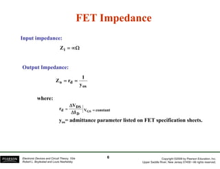
- 6. FET Impedance Input impedance: p Zi = Ōł×╬® Output Impedance: Z = r = 1 o d y yos ╬öV where: ╬ö d I GS V constant DS D V r = = ╬ö yos= admittance parameter listed on FET specification sheets. Copyright ┬®2009 by Pearson Education, Inc. Upper Saddle River, New Jersey 07458 ŌĆó All rights reserved. Electronic Devices and Circuit Theory, 10/e Robert L. Boylestad and Louis Nashelsky 6
- 7. FET AC Equivalent Circuit Copyright ┬®2009 by Pearson Education, Inc. Upper Saddle River, New Jersey 07458 ŌĆó All rights reserved. Electronic Devices and Circuit Theory, 10/e Robert L. Boylestad and Louis Nashelsky 7
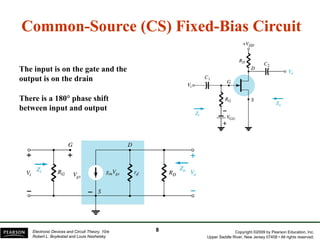
- 8. Common-Source (CS) Fixed-Bias Circuit The input is on the gate and the output is on the drain There is a 180┬░ phase shift between input and output Copyright ┬®2009 by Pearson Education, Inc. Upper Saddle River, New Jersey 07458 ŌĆó All rights reserved. Electronic Devices and Circuit Theory, 10/e Robert L. Boylestad and Louis Nashelsky 8
- 9. Calculations Input impedance: Zi = RG p Output p impedance: Zo = RD || rd Z R o D r Ōēź 10R d D Ōēģ Voltage gain: o A m d D g (r || R ) V v = = ŌłÆ V i v g R rd 10RD m D o V i V A = = ŌłÆ Ōēź Copyright ┬®2009 by Pearson Education, Inc. Upper Saddle River, New Jersey 07458 ŌĆó All rights reserved. Electronic Devices and Circuit Theory, 10/e Robert L. Boylestad and Louis Nashelsky 9
- 10. Common-Source (CS) Self-Bias Circuit This is a common-source amplifier configuration, so the input is on the gate and the output is on the drain There is a 180┬░ phase shift between input and output Copyright ┬®2009 by Pearson Education, Inc. Upper Saddle River, New Jersey 07458 ŌĆó All rights reserved. Electronic Devices and Circuit Theory, 10/e Robert L. Boylestad and Louis Nashelsky 10
- 11. Calculations Input impedance: Z Zi = R RG p Output p impedance: Zo = rd || RD Z R o D r Ōēź 10R d D Ōēģ Voltage gain: Av = ŌłÆgm(rd || RD) Av = ŌłÆ gmRD rd Ōēź 10RD Copyright ┬®2009 by Pearson Education, Inc. Upper Saddle River, New Jersey 07458 ŌĆó All rights reserved. Electronic Devices and Circuit Theory, 10/e Robert L. Boylestad and Louis Nashelsky 11
- 12. Common-Source (CS) Self-Bias Circuit Removing Cs affects the gain of the circuit. Copyright ┬®2009 by Pearson Education, Inc. Upper Saddle River, New Jersey 07458 ŌĆó All rights reserved. Electronic Devices and Circuit Theory, 10/e Robert L. Boylestad and Louis Nashelsky 12
- 13. Calculations Input impedance: Zi i = G RG Output impedance: Z R Ōēź o D r 10R d D Ōēģ Voltage gain: Vo gmRD A = = ŌłÆ R R D S d m S i v r V 1 g R + + + Vo o m gmRD D A r 10(R R ) v 1 g R d D S m S i g V Ōēź + + = = ŌłÆ Copyright ┬®2009 by Pearson Education, Inc. Upper Saddle River, New Jersey 07458 ŌĆó All rights reserved. Electronic Devices and Circuit Theory, 10/e Robert L. Boylestad and Louis Nashelsky 13
- 14. Common-Source (CS) Voltage-Divider Bias This is a common-source amplifier configuration, so the input is on the gate and the output is on the drain. Copyright ┬®2009 by Pearson Education, Inc. Upper Saddle River, New Jersey 07458 ŌĆó All rights reserved. Electronic Devices and Circuit Theory, 10/e Robert L. Boylestad and Louis Nashelsky 14
- 15. Impedances Input impedance: Zi = R1 || R2 Output impedance: Zo = rd || RD Z R Ōēź o D r 10R d D Ōēģ Voltage gain: Av = ŌłÆgm(rd || RD ) Av = ŌłÆ gmRD rd Ōēź 10RD Copyright ┬®2009 by Pearson Education, Inc. Upper Saddle River, New Jersey 07458 ŌĆó All rights reserved. Electronic Devices and Circuit Theory, 10/e Robert L. Boylestad and Louis Nashelsky 15
- 16. Source Follower (Common-Drain) Circuit In a common-drain amplifier configuration, the input is on the gate, but the output is from the source. There is no phase shift between input and output. Copyright ┬®2009 by Pearson Education, Inc. Upper Saddle River, New Jersey 07458 ŌĆó All rights reserved. Electronic Devices and Circuit Theory, 10/e Robert L. Boylestad and Louis Nashelsky 16
- 17. Impedances Input impedance: Z Zi = R RG Output impedance: Z = r || R || 1 m o d S g 1 Z R || Ōēģ Ōēź rd 10RS m o S g Voltage g (r || R ) m d S gain: = = v + 1 g (r || R ) V o V A m d S i V A = = + Ōēź v 1 g R d r 10 m S m S o i g R V Copyright ┬®2009 by Pearson Education, Inc. Upper Saddle River, New Jersey 07458 ŌĆó All rights reserved. Electronic Devices and Circuit Theory, 10/e Robert L. Boylestad and Louis Nashelsky 17
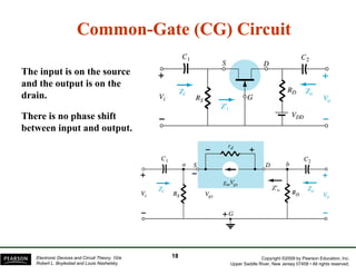
- 18. Common-Gate (CG) Circuit The input is on the source and the output is on the drain. There is no phase shift between input and output. Copyright ┬®2009 by Pearson Education, Inc. Upper Saddle River, New Jersey 07458 ŌĆó All rights reserved. Electronic Devices and Circuit Theory, 10/e Robert L. Boylestad and Louis Nashelsky 18
- 19. Calculations Input impedance: ŌÄż ŌÄźŌÄ” ŌÄĪ + ŌÄóŌÄŻ r + R = d D i S 1 g r m d Z R || 1 Z R || Ōēģ Ōēź rd 10RD m i S g Output impedance: Zo = RD || rd Voltage o D rd 10 Z Ōēģ R Ōēź ŌÄż ŌÄźŌÄ” ŌÄĪ ŌÄó ŌÄŻ + D R = = ŌÄ” A d v = m D rd Ōēź 10RD g R m D gain: o r V A g R ŌÄż ŌÄźŌÄ” ŌÄĪ + ŌÄóŌÄŻ D R d i v r 1 V Copyright ┬®2009 by Pearson Education, Inc. Upper Saddle River, New Jersey 07458 ŌĆó All rights reserved. Electronic Devices and Circuit Theory, 10/e Robert L. Boylestad and Louis Nashelsky 19
- 20. D-Type MOSFET AC Equivalent Copyright ┬®2009 by Pearson Education, Inc. Upper Saddle River, New Jersey 07458 ŌĆó All rights reserved. Electronic Devices and Circuit Theory, 10/e Robert L. Boylestad and Louis Nashelsky 20
- 21. E-Type MOSFETAC Equivalent gm and rd can be found in the specification sheet for the FET. Copyright ┬®2009 by Pearson Education, Inc. Upper Saddle River, New Jersey 07458 ŌĆó All rights reserved. Electronic Devices and Circuit Theory, 10/e Robert L. Boylestad and Louis Nashelsky 21
- 22. Common-Source Drain-Feedback There is a 180┬░ phase shift between input and output. Copyright ┬®2009 by Pearson Education, Inc. Upper Saddle River, New Jersey 07458 ŌĆó All rights reserved. Electronic Devices and Circuit Theory, 10/e Robert L. Boylestad and Louis Nashelsky 22
- 23. Calculations Input impedance: R r || R F d D 1 g (r || R ) Z m d D i + + = R ||R 10R F i R Z Ōēģ Ōēź RF rd RD ,rd 10RD >> + 1 g R m D Output impedance: p p Zo = RF || rd ||RD Zo Ōēģ RD RF >>rd || RD , rd Ōēź10RF d D d D Voltage gain: Av = ŌłÆgm(RF || rd || RD ) Av Ōēģ ŌłÆgmRD RF>>rd||RD,rdŌēź10RD Copyright ┬®2009 by Pearson Education, Inc. Upper Saddle River, New Jersey 07458 ŌĆó All rights reserved. Electronic Devices and Circuit Theory, 10/e Robert L. Boylestad and Louis Nashelsky 23
- 24. Common-Source Voltage-Divider Bias Copyright ┬®2009 by Pearson Education, Inc. Upper Saddle River, New Jersey 07458 ŌĆó All rights reserved. Electronic Devices and Circuit Theory, 10/e Robert L. Boylestad and Louis Nashelsky 24
- 25. Calculations Input impedance: Zi=R1|| R2 O t Output t i d impedance: Zo = rd || RD Zo RD rd 10 Z Ōēģ R Ōēź Voltage gain: Av = ŌłÆgm(rd || RD) A Ōēģ g R Av ŌłÆgmRD rd Ōēź10RD Copyright ┬®2009 by Pearson Education, Inc. Upper Saddle River, New Jersey 07458 ŌĆó All rights reserved. Electronic Devices and Circuit Theory, 10/e Robert L. Boylestad and Louis Nashelsky 25
- 26. Summary Table Copyright ┬®2009 by Pearson Education, Inc. Upper Saddle River, New Jersey 07458 ŌĆó All rights reserved. Electronic Devices and Circuit Theory, 10/e Robert L. Boylestad and Louis Nashelsky moreŌĆ” 26
- 27. Summary Table Copyright ┬®2009 by Pearson Education, Inc. Upper Saddle River, New Jersey 07458 ŌĆó All rights reserved. Electronic Devices and Circuit Theory, 10/e Robert L. Boylestad and Louis Nashelsky 27
- 28. Troubleshooting Check the DC bias voltages: If not correct check power supply, resistors, FET. Also check to ensure that the coupling capacitor between amplifier stages is OK. . Check the AC voltages: If not correct check FET, capacitors and the loading effect of the next stage Copyright ┬®2009 by Pearson Education, Inc. Upper Saddle River, New Jersey 07458 ŌĆó All rights reserved. Electronic Devices and Circuit Theory, 10/e Robert L. Boylestad and Louis Nashelsky 28
- 29. Practical Applications Three-Channel Audio Mixer Silent Switching Phase Shift Networks Motion Detection System Copyright ┬®2009 by Pearson Education, Inc. Upper Saddle River, New Jersey 07458 ŌĆó All rights reserved. Electronic Devices and Circuit Theory, 10/e Robert L. Boylestad and Louis Nashelsky 29