狠狠撸

狠狠撸Share a Scribd company logo
UNIT -6
SAMPLING GATES
AND
LOGIC FAMILIES
Sampling Gates
? Sampling Gates are also called as Transmission gates,linear
gates and selection circuits,in which the output is exact
reproduction of the input during a selected time intervaland
zero otherwise.
? It has two inputs – gating signal, rectangular wave
? Twotypes
? Unidirectional
? Bidirectional
Gating
Input
Sampling Gate
Output
Principle of operation of a linear gate:
? Principle of operation of a linear gate: Lineargates
can use (a) a series switch or (b) a shunt switchfig
Unidirectional Gate
? unidirectional sampling gates are those which transmit signals of only one
polarity(i.e,. either positive ornegative)
? The gating signal is also known as control pulse, selector pulse or an
enabling pulse. It is a negative signal, the magnitude of which changes
abruptly between –V2 and –V1.
Unidirectional gate
? Consider the instant at which the gate signal is –V1 which is a reasonably
large negative voltage. Even if an input pulse is present at this time instant,
the diode remains OFF as the input pulse amplitude may not be sufficiently
large so as to forward bias it. Hence there is no output. Now consider the
duration when the gate signal has a value –V2 and when the input is also
present (coincidence occurs).
Output waveform
? When the control signal shifted toupward
pedestal
? When the control signal is shifted to positive value ,so it willbe
superimposed on input and control signals .so the pedestal
occurs
Unidirectional diode coincidence gate
? When any of the control
voltages is at –V1, point X is
at a large negative voltage,
even if the input pulse Vs is
present., D0 is reverse biased.
Hence there is no signal atthe
output.
? When all the control voltages,
on the other hand, are at –V2 ,
if an input signal Vs ispresent,
D0 is forward biased and the
output is a pulse of 5V
.Hence
this circuit is a coincidence
circuit or ANDcircuit.
Bidirectional Sampling gate
? Bidirectional sampling gates are those which transmit
signals of both the polarities.
Bidirectional Sampling gate using
Transistor
? Bidirectional sampling gates are those which transmit signals of both thepolarities.
Circuit that minimizes the
pedestal
? Circuit that minimizes the pedestal
Contd …
? The control signal applied to the base of Q2 is of opposite polarity to that applied to
the base of Q1. When the gating signal connected to Q1 is negative, Q1 is OFF and at
the same time the gating signal connected to Q2 drives Q2 ON and draws current IC.
As a result there is a dc voltage Vdc at the collector. But when the gate voltage at the
base of Q1 drives Q1 ON, Q2 goes OFF. But during this gate period if the input signal
is present, it is amplified and is available at the output, with phase inversion. But the
dc reference level practically is Vdc. As such the pedestal is either eliminated or
minimized.
Two Diode Sampling gate
? When the control signals are at V1, D1 and D2 are OFF,no input signal is
transmitted to the output. But when control signals are at V2, diode D1
conducts if the input is positive pulses and diode D2 conducts if the input is
negative pulses. Hence these bidirectional inputs are transmitted to the
output. This arrangement eliminates pedestal, because of the circuit
symmetry.
Four Diode Sampling gate
? When the control signals are at V1, D1 and D2 are OFF,no input
signal is transmitted to the output. But when control signals areat
V2, diode D1 conducts if the input is positive pulses and diode D2
conducts if the input is negative pulses. Hence these bidirectional
inputs are transmitted to the output. This arrangement eliminates
pedestal, because of the circuitsymmetry.
Applications
? ChopperAmplifier
? Multiplexers
? ADC
? Sampling Scope
? Sample and hold circuits
Chopper Amplifier
? Sometimes it becomes necessary to amplify a signal v that has very small
dv/dt and that the amplitude of the signal itself is very small, typically of the
order of millivolts. Neither, ac amplifiers using large coupling condensers
nor dc amplifiers with the associated drift would be useful for such an
application. A chopper stabilized amplifier employing sampling gates canbe
a useful choice in such a applications
REALIZATION OF LOGIC GATES
USING DIODES AND TRANSISTORS
? OR GATE
? OR GATEPERFORMS LOGICALADDITION.
? THE OR OPERATOR IS INDICATED BYAPLUS (+)
SIGN.
OR GATE USING DIODES
OPERATION:
?ASSUME THE
INPUTVOLTAGES
ARE EITHER 0V
(LOW) OR 5V
(HIGH).
BOTHAAND BARE
LOW:
?THE DIODES ARE
OFF AND WE CAN
REPLACE THE
Contd.
AIS LOWAND B ISHIGH:
? WHENAIS LOWTHE CORRESPONDING DIODE WILLBE OFFAND,
B IS HIGH SO THE DIODE CORRESPONDS TO THE INPUT B WILL
BE ON.
? NOW WE CAN REPLACE THE ON DIODE BY THE SHORTCIRCUIT
EQUIVALENTAND THE OUTPUTC=5V.
? B IS LOWANDAIS HIGH:
? WHEN B IS LOW THE CORRESPONDING DIODE WILL BE OFFAND,
A IS HIGH SO THE DIODE CORRESPONDS TO THE INPUT A WILL
BE ON.
? NOW WE CAN REPLACE THE ON DIODE BY THE SHORTCIRCUIT
EQUIVALENTAND THE OUTPUTC=5V.
? BOTHAAND BARE HIGH:
? WHEN BOTH THE INPUTSARE HIGH BOTH THE DIODES WILLBE
ON AND THE OUTPUTC=5V.
AND Gate
? THE AND GATEPERFORMSLOGICAL
MULTIPLICATION.
? THE AND OPERATOR IS INDICATED BY USINGADOT
(.) SIGN OR BY NOT SHOWING ANY OPERATOR
SYMBOLATALL.
AND GATE USING DIODES
? ASSUME THE INPUT VOLTAGESARE EITHER 0V (LOW) OR5V
(HIGH).
BOTH AAND BARE LOW:
o WHEN BOTHAAND BARE LOW BOTH THE DIODESARE
ON AND WE CAN REPLACE THE DIODES BY SHORT
CIRCUIT EQUIVALENT.
o HENCE POINT X IS CONNECTED TO GROUND AND OUTPUT
C = 0V.
o A IS LOWAND B IS HIGH:
o WHEN A IS LOW THE CORRESPONDING DIODE WILL BE ON
AND, B IS HIGH SO THE DIODE CORRESPONDS TO THE INPUT
B WILL BEOFF.
o NOW WE CAN REPLACE THE ON DIODE BY THE SHORT
CIRCUIT EQUIVALENT; HENCE POINT X IS CONNECTED TO
GROUND AND THE OUTPUTC=0V.
Contd.
B IS LOWANDAIS HIGH:
o WHEN B IS LOW THE CORRESPONDING DIODE
WILL BE ON AND, A IS HIGH SO THE DIODE
CORRESPONDS TO THE INPUT AWILL BEOFF.
o NOW WE CAN REPLACE THE ON DIODE BY THE
SHORT CIRCUIT EQUIVALENT; HENCE POINT X
IS CONNECTED TO GROUND AND THE OUTPUT
C=0V.
BOTHAAND BARE HIGH:
o BOTH THE DIODES WILLBE OFFAND THE
OUTPUTC=5V.
NOT GATE(INVERTER)
? THE OUTPUT OFANOT GATEIS THECOMPLEMENT
OF THE INPUT.
? THE BUBBLE REPRESENTS INVERSION OR
COMPLEMENT.
REALIZATION OF NOT GATE
USING TRANSISTOR
A ISHIGH:
o When +5v is applied to a, the
transistor will be fully on.
o So maximum collector
current will flow and vcc
=icr, making vc or voltage at
point b as zero. [Recall ce
loop kvl: vc=vcc-icr].
o A IS LOW:
When 0v is applied to a, the
transistor will be cut-off.
So ic=0ma and vc or voltage
at point b is equal to vcc.
Logic Families Vocabulary
TTL (Transistor Transistor Logic) Integrated-circuit technology thatuses
the bipolar transistor as the principal circuitelement.
CMOS (Complimentary Metal Oxide Semiconductor) Integrated-circuit
technology that uses the field-effect transistor as the principal circuit element.
ECL (Emitter Coupled Logic) Integrated-circuit technology that uses the bipolar
transistors configured as a differential amplifier. This eliminates saturation and
improves speed but uses more power than other families.
OTHER DIGITAL IC SPECIFICATIONS
? Drive Capabilities- sometimes referred to as fan-in or fan-out.
? Fan out- number of inputs of a logic family that can be driven
by a single output. The drive capability of outputs.
? Fan in- the load an input places on an output.
? Propagation delay- has to do with the “speed” of the logic
element. Lower propagation delays mean higher speed which
is a desirable characteristic.
? Power Dissipation- generally, as propagation delays decrease,
power consumption and heat generation increase. CMOS is
noted for low power consumption.
Fanout: the maximum number of logic inputs (of thesame
logic family) that an output can drivereliably
Logic families: fanout
I
DC fanout = min( OH , )
IIH IIL
IOL
147
Logic families: propagation
delay
TPD,HL TPD,LH
TPD,HL – input-to-output propagation delay from HI to LO output
TPD,LH – input-to-output propagation delay from LO to HIoutput
Speed-power product: TPD ? Pavg
148
Logic families: noise margin
VNH
VNL
HI state noise margin:
VNH = VOH(min) –VIH(min)
LO state noise margin:
VNL = VIL(max) – VOL(max)
Noise margin:
VN = min(VNH,VNL)
149
TOTEM POLE NAND GATE
? First introduced by in
1964 (Texas
Instruments)
? TTL has shaped
digital technology in
many ways
? Standard TTLfamily
(e.g. 7400) is obsolete
? Newer TTLfamilies
still
used (e.g.
74ALS00)
Open collector gate
? An open collector is a common type of output found on many integrated
circuits(IC).
? Instead of outputting a signal of a specific voltage or current, the output
signal is applied to the base of an internal NPN transistor whose collector
is externalized (open) on a pin of the IC. The emitter of the transistor is
connected internally to the ground pin. If the output device is
a MOSFET the output is called open drain and it functions in a similar
way.
Tristate TTL
? Tristate means a state of logic other than ?1?and ?0?
in which there is a high impedance state and there is
no isource or isink at the output stage transistor (or
MOSFET). A gate capable of being in ?1?,?0?and
tristate is known as tristategate
Direct-coupled transistor
logic (DCTL)
? Direct-coupled transistor logic (DCTL) is similar to resistor–
transistor logic (RTL) but the input transistor bases are connected
directly to the collector outputs without any base resistors.
Consequently, DCTL gates have fewer components, are more
economical, and are simpler to fabricate onto integrated circuits
than RTL gates. Unfortunately, DCTL has much smaller signal
levels, has more susceptibility to ground noise, and requires
matched transistor characteristics. The transistors are also heavily
overdriven; that is a good feature in that it reduces the saturation
voltage of the output transistors, but it also slows the circuit down
due to a high stored charge in the base.[1] Gate fan-out is limited
due to "current hogging": if the transistor base-emitter voltages
(VBE) are not well matched, then the base-emitter junction of one
transistor may conduct most of the input drive current at such a
low base-emitter voltage that other input transistors fail to turn on
ECL
Emitter-Coupled Logic (ECL)
?PROS: Fastest logic family available(~1ns)
? CONS: low noise margin and high power dissipation
?Operated in emitter coupled geometry (recall
differential amplifier or emitter-follower), transistors
are biased and operate near their Q-point (nevernear
saturation!)
? Logic levels. “0”: –1.7V. “1”: –0.8V
? Such strange logic levels require extra effort when
interfacing to TTL/CMOS logicfamilies.
? Open LTspice example: ECLinverter…
154
ECL
EMITTER COUPLED LOGIC
LOGIC FAMILIESAND
INTRODUCTION
? WE HVE SEEN THATDIFFERENT DEVICES USE
DIFFERENT VOLTAGES RANGES FOR THEIR LOGIC
LEVELS.
? THEY ALSO DIFFER IN OTHER CHARACTERISTICE
? IN ORDER TOASSURE CORRECT OPERATIONWHEN
GATESARE INTERCONNECTED THEY ARE
NORMALLYPRODUCED IN LOGIC FAMILIES
? THE MOSTLYWIDELYUSED FAMILIESARE
– COMPLEMENTARY METAL OXIDE(CMOS)
– TRANSISTOR- TRANSISTOR LOGIC (TTL)
– EMITTER COUPLED LOGIG (ECL)
COPARISON OF LOGIC FAMILIES

More Related Content

Similar to Engeneering Model Traffic Lights Circuit (20)

Transistor as a switch
Transistor as a switch Transistor as a switch
Transistor as a switch
jignesh prajapati
?
UNIT - 6.pdf
UNIT - 6.pdfUNIT - 6.pdf
UNIT - 6.pdf
bt2O1O5134KaranGupta
?
UNIT 3.pptx
UNIT 3.pptxUNIT 3.pptx
UNIT 3.pptx
ssuser022fec
?
Unit I.pptx
Unit I.pptxUnit I.pptx
Unit I.pptx
anupvibhute3
?
10 lm 555 timer
10 lm 555 timer10 lm 555 timer
10 lm 555 timer
Md. Khairul Alam t@ifur
?
Lica unit4 ppt
Lica unit4 ppt Lica unit4 ppt
Lica unit4 ppt
elakkia8
?
Operational Amplifire.pptx
Operational Amplifire.pptxOperational Amplifire.pptx
Operational Amplifire.pptx
ProfVilasShamraoPati
?
Integrated Circuit
Integrated CircuitIntegrated Circuit
Integrated Circuit
Nabil Nader
?
Unit-6 ae 3rd sem by Prof Priyanka Jain.pptx
Unit-6 ae 3rd sem by Prof Priyanka Jain.pptxUnit-6 ae 3rd sem by Prof Priyanka Jain.pptx
Unit-6 ae 3rd sem by Prof Priyanka Jain.pptx
amitthory13012003
?
Schmitt trigger circuit
Schmitt trigger circuitSchmitt trigger circuit
Schmitt trigger circuit
taranjeet10
?
programmableasici-160912165934 ac and dc io
programmableasici-160912165934 ac and dc ioprogrammableasici-160912165934 ac and dc io
programmableasici-160912165934 ac and dc io
423ec0007
?
Diode Application
Diode ApplicationDiode Application
Diode Application
UMAR ALI
?
Data converter fundamentals
Data converter fundamentalsData converter fundamentals
Data converter fundamentals
Abhishek Kadam
?
Logic families ppt eceb srp
Logic families ppt eceb srpLogic families ppt eceb srp
Logic families ppt eceb srp
Saikat Dutt
?
Logic Gates & Family.pdf
Logic Gates & Family.pdfLogic Gates & Family.pdf
Logic Gates & Family.pdf
DanishKhan313548
?
Logic not gate tutorial with logic gate truth table
Logic not gate tutorial with logic gate truth tableLogic not gate tutorial with logic gate truth table
Logic not gate tutorial with logic gate truth table
guru nanak institute of technology
?
Diode Applications.pptx
Diode Applications.pptxDiode Applications.pptx
Diode Applications.pptx
ShrutiSharma485933
?
OP AMP Applications
OP AMP ApplicationsOP AMP Applications
OP AMP Applications
aroosa khan
?
3.4.Clipper,clamper,peak detector.ppt
3.4.Clipper,clamper,peak detector.ppt3.4.Clipper,clamper,peak detector.ppt
3.4.Clipper,clamper,peak detector.ppt
NANDHAKUMARA10
?
Clippers_and_Clampers.pptx
Clippers_and_Clampers.pptxClippers_and_Clampers.pptx
Clippers_and_Clampers.pptx
SIVA NAGI REDY KALLI
?

Recently uploaded (20)

Professional Frozen Beverage Maker: IFSM26SERIES_WL_TRI_Recipe Book
Professional Frozen Beverage Maker: IFSM26SERIES_WL_TRI_Recipe BookProfessional Frozen Beverage Maker: IFSM26SERIES_WL_TRI_Recipe Book
Professional Frozen Beverage Maker: IFSM26SERIES_WL_TRI_Recipe Book
NathanBaughman3
?
加拿大毕业证购买(魁北克大学成绩单)鲍蚕础惭文凭学历认证
加拿大毕业证购买(魁北克大学成绩单)鲍蚕础惭文凭学历认证加拿大毕业证购买(魁北克大学成绩单)鲍蚕础惭文凭学历认证
加拿大毕业证购买(魁北克大学成绩单)鲍蚕础惭文凭学历认证
taqyed
?
727381415-SQUID-GAME-POWERPOINT-CLASSROOM-INTERACTIVE-POWERPOINT-GAME.pptx
727381415-SQUID-GAME-POWERPOINT-CLASSROOM-INTERACTIVE-POWERPOINT-GAME.pptx727381415-SQUID-GAME-POWERPOINT-CLASSROOM-INTERACTIVE-POWERPOINT-GAME.pptx
727381415-SQUID-GAME-POWERPOINT-CLASSROOM-INTERACTIVE-POWERPOINT-GAME.pptx
rossanthonytan130
?
3Copy of Jerez_Izabella_DMBS_2024-10.pdf
3Copy of Jerez_Izabella_DMBS_2024-10.pdf3Copy of Jerez_Izabella_DMBS_2024-10.pdf
3Copy of Jerez_Izabella_DMBS_2024-10.pdf
jerezbellav
?
2- 8-Point Action Agenda_ The Medium-Term Strategy of the Health Sector for 2...
2- 8-Point Action Agenda_ The Medium-Term Strategy of the Health Sector for 2...2- 8-Point Action Agenda_ The Medium-Term Strategy of the Health Sector for 2...
2- 8-Point Action Agenda_ The Medium-Term Strategy of the Health Sector for 2...
NashiedaLilangBuale
?
Download GRAPHISOFT ArchiCAD Crack 28.1.0.4001 Full Version 2025
Download GRAPHISOFT ArchiCAD Crack 28.1.0.4001 Full Version 2025Download GRAPHISOFT ArchiCAD Crack 28.1.0.4001 Full Version 2025
Download GRAPHISOFT ArchiCAD Crack 28.1.0.4001 Full Version 2025
am2612067
?
Template to build an outstanding presentation
Template to build an outstanding presentationTemplate to build an outstanding presentation
Template to build an outstanding presentation
priyankaarul2023
?
oresent simple and continuous classes en un
oresent simple and continuous classes en unoresent simple and continuous classes en un
oresent simple and continuous classes en un
AlejandraQusyo
?
Electromyography_Based_Decoding_of_Dexterous_In-Hand_Manipulation_Motions_Wit...
Electromyography_Based_Decoding_of_Dexterous_In-Hand_Manipulation_Motions_Wit...Electromyography_Based_Decoding_of_Dexterous_In-Hand_Manipulation_Motions_Wit...
Electromyography_Based_Decoding_of_Dexterous_In-Hand_Manipulation_Motions_Wit...
annupriya1295
?
Mike Hydes LinkedIn Profile (Backup)
Mike Hydes LinkedIn Profile (Backup)Mike Hydes LinkedIn Profile (Backup)
Mike Hydes LinkedIn Profile (Backup)
Mike Hydes
?
neurology neoplasm tumors and cysts part 2
neurology neoplasm tumors and cysts part 2neurology neoplasm tumors and cysts part 2
neurology neoplasm tumors and cysts part 2
shivangilahoty56
?
2025 Resume: Rebecca Sage, Communicator, Designer, Analyst
2025 Resume: Rebecca Sage, Communicator, Designer, Analyst2025 Resume: Rebecca Sage, Communicator, Designer, Analyst
2025 Resume: Rebecca Sage, Communicator, Designer, Analyst
Rebecca Sage
?
How to Land an IT Job From Non-Tech Fields in 2025
How to Land an IT Job From Non-Tech Fields in 2025How to Land an IT Job From Non-Tech Fields in 2025
How to Land an IT Job From Non-Tech Fields in 2025
Base Camp
?
FSU COSSPP Engage Magazine 2022-2023 - page view
FSU COSSPP Engage Magazine 2022-2023 - page viewFSU COSSPP Engage Magazine 2022-2023 - page view
FSU COSSPP Engage Magazine 2022-2023 - page view
Rebecca Sage
?
Best Crypto Analysts: Insights from Top Blockchain Experts
Best Crypto Analysts: Insights from Top Blockchain ExpertsBest Crypto Analysts: Insights from Top Blockchain Experts
Best Crypto Analysts: Insights from Top Blockchain Experts
cryptoanalyst37
?
VT VT VT VT VT VT VT VT VR VT VT VT VT VT
VT VT VT VT VT VT VT VT VR VT VT VT VT VTVT VT VT VT VT VT VT VT VR VT VT VT VT VT
VT VT VT VT VT VT VT VT VR VT VT VT VT VT
syam268254
?
Contemporaries_10446988.pdf to learning and inovation
Contemporaries_10446988.pdf to learning and inovationContemporaries_10446988.pdf to learning and inovation
Contemporaries_10446988.pdf to learning and inovation
kumarmritunjay1580
?
一比一原版(鲍罢厂骋毕业证书)多伦多大学毕业证如何办理
一比一原版(鲍罢厂骋毕业证书)多伦多大学毕业证如何办理一比一原版(鲍罢厂骋毕业证书)多伦多大学毕业证如何办理
一比一原版(鲍罢厂骋毕业证书)多伦多大学毕业证如何办理
taqyed
?
ibp_final_ppts_3[1].pptxggggggggggggggggggggggggggggggggggggggggggggggggggggg...
ibp_final_ppts_3[1].pptxggggggggggggggggggggggggggggggggggggggggggggggggggggg...ibp_final_ppts_3[1].pptxggggggggggggggggggggggggggggggggggggggggggggggggggggg...
ibp_final_ppts_3[1].pptxggggggggggggggggggggggggggggggggggggggggggggggggggggg...
MobasshiraHaqueOishi2
?
How to Prepare for Palo Alto NGFW-Engineer Certification?
How to Prepare for Palo Alto NGFW-Engineer Certification?How to Prepare for Palo Alto NGFW-Engineer Certification?
How to Prepare for Palo Alto NGFW-Engineer Certification?
NWEXAM
?
Professional Frozen Beverage Maker: IFSM26SERIES_WL_TRI_Recipe Book
Professional Frozen Beverage Maker: IFSM26SERIES_WL_TRI_Recipe BookProfessional Frozen Beverage Maker: IFSM26SERIES_WL_TRI_Recipe Book
Professional Frozen Beverage Maker: IFSM26SERIES_WL_TRI_Recipe Book
NathanBaughman3
?
加拿大毕业证购买(魁北克大学成绩单)鲍蚕础惭文凭学历认证
加拿大毕业证购买(魁北克大学成绩单)鲍蚕础惭文凭学历认证加拿大毕业证购买(魁北克大学成绩单)鲍蚕础惭文凭学历认证
加拿大毕业证购买(魁北克大学成绩单)鲍蚕础惭文凭学历认证
taqyed
?
727381415-SQUID-GAME-POWERPOINT-CLASSROOM-INTERACTIVE-POWERPOINT-GAME.pptx
727381415-SQUID-GAME-POWERPOINT-CLASSROOM-INTERACTIVE-POWERPOINT-GAME.pptx727381415-SQUID-GAME-POWERPOINT-CLASSROOM-INTERACTIVE-POWERPOINT-GAME.pptx
727381415-SQUID-GAME-POWERPOINT-CLASSROOM-INTERACTIVE-POWERPOINT-GAME.pptx
rossanthonytan130
?
3Copy of Jerez_Izabella_DMBS_2024-10.pdf
3Copy of Jerez_Izabella_DMBS_2024-10.pdf3Copy of Jerez_Izabella_DMBS_2024-10.pdf
3Copy of Jerez_Izabella_DMBS_2024-10.pdf
jerezbellav
?
2- 8-Point Action Agenda_ The Medium-Term Strategy of the Health Sector for 2...
2- 8-Point Action Agenda_ The Medium-Term Strategy of the Health Sector for 2...2- 8-Point Action Agenda_ The Medium-Term Strategy of the Health Sector for 2...
2- 8-Point Action Agenda_ The Medium-Term Strategy of the Health Sector for 2...
NashiedaLilangBuale
?
Download GRAPHISOFT ArchiCAD Crack 28.1.0.4001 Full Version 2025
Download GRAPHISOFT ArchiCAD Crack 28.1.0.4001 Full Version 2025Download GRAPHISOFT ArchiCAD Crack 28.1.0.4001 Full Version 2025
Download GRAPHISOFT ArchiCAD Crack 28.1.0.4001 Full Version 2025
am2612067
?
Template to build an outstanding presentation
Template to build an outstanding presentationTemplate to build an outstanding presentation
Template to build an outstanding presentation
priyankaarul2023
?
oresent simple and continuous classes en un
oresent simple and continuous classes en unoresent simple and continuous classes en un
oresent simple and continuous classes en un
AlejandraQusyo
?
Electromyography_Based_Decoding_of_Dexterous_In-Hand_Manipulation_Motions_Wit...
Electromyography_Based_Decoding_of_Dexterous_In-Hand_Manipulation_Motions_Wit...Electromyography_Based_Decoding_of_Dexterous_In-Hand_Manipulation_Motions_Wit...
Electromyography_Based_Decoding_of_Dexterous_In-Hand_Manipulation_Motions_Wit...
annupriya1295
?
Mike Hydes LinkedIn Profile (Backup)
Mike Hydes LinkedIn Profile (Backup)Mike Hydes LinkedIn Profile (Backup)
Mike Hydes LinkedIn Profile (Backup)
Mike Hydes
?
neurology neoplasm tumors and cysts part 2
neurology neoplasm tumors and cysts part 2neurology neoplasm tumors and cysts part 2
neurology neoplasm tumors and cysts part 2
shivangilahoty56
?
2025 Resume: Rebecca Sage, Communicator, Designer, Analyst
2025 Resume: Rebecca Sage, Communicator, Designer, Analyst2025 Resume: Rebecca Sage, Communicator, Designer, Analyst
2025 Resume: Rebecca Sage, Communicator, Designer, Analyst
Rebecca Sage
?
How to Land an IT Job From Non-Tech Fields in 2025
How to Land an IT Job From Non-Tech Fields in 2025How to Land an IT Job From Non-Tech Fields in 2025
How to Land an IT Job From Non-Tech Fields in 2025
Base Camp
?
FSU COSSPP Engage Magazine 2022-2023 - page view
FSU COSSPP Engage Magazine 2022-2023 - page viewFSU COSSPP Engage Magazine 2022-2023 - page view
FSU COSSPP Engage Magazine 2022-2023 - page view
Rebecca Sage
?
Best Crypto Analysts: Insights from Top Blockchain Experts
Best Crypto Analysts: Insights from Top Blockchain ExpertsBest Crypto Analysts: Insights from Top Blockchain Experts
Best Crypto Analysts: Insights from Top Blockchain Experts
cryptoanalyst37
?
VT VT VT VT VT VT VT VT VR VT VT VT VT VT
VT VT VT VT VT VT VT VT VR VT VT VT VT VTVT VT VT VT VT VT VT VT VR VT VT VT VT VT
VT VT VT VT VT VT VT VT VR VT VT VT VT VT
syam268254
?
Contemporaries_10446988.pdf to learning and inovation
Contemporaries_10446988.pdf to learning and inovationContemporaries_10446988.pdf to learning and inovation
Contemporaries_10446988.pdf to learning and inovation
kumarmritunjay1580
?
一比一原版(鲍罢厂骋毕业证书)多伦多大学毕业证如何办理
一比一原版(鲍罢厂骋毕业证书)多伦多大学毕业证如何办理一比一原版(鲍罢厂骋毕业证书)多伦多大学毕业证如何办理
一比一原版(鲍罢厂骋毕业证书)多伦多大学毕业证如何办理
taqyed
?
ibp_final_ppts_3[1].pptxggggggggggggggggggggggggggggggggggggggggggggggggggggg...
ibp_final_ppts_3[1].pptxggggggggggggggggggggggggggggggggggggggggggggggggggggg...ibp_final_ppts_3[1].pptxggggggggggggggggggggggggggggggggggggggggggggggggggggg...
ibp_final_ppts_3[1].pptxggggggggggggggggggggggggggggggggggggggggggggggggggggg...
MobasshiraHaqueOishi2
?
How to Prepare for Palo Alto NGFW-Engineer Certification?
How to Prepare for Palo Alto NGFW-Engineer Certification?How to Prepare for Palo Alto NGFW-Engineer Certification?
How to Prepare for Palo Alto NGFW-Engineer Certification?
NWEXAM
?

Engeneering Model Traffic Lights Circuit

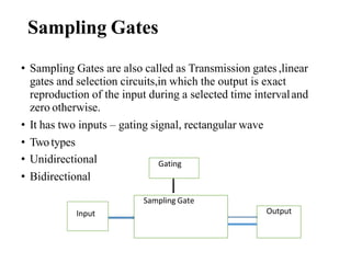
  • 2. Sampling Gates ? Sampling Gates are also called as Transmission gates,linear gates and selection circuits,in which the output is exact reproduction of the input during a selected time intervaland zero otherwise. ? It has two inputs – gating signal, rectangular wave ? Twotypes ? Unidirectional ? Bidirectional Gating Input Sampling Gate Output
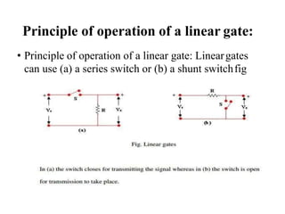
  • 3. Principle of operation of a linear gate: ? Principle of operation of a linear gate: Lineargates can use (a) a series switch or (b) a shunt switchfig
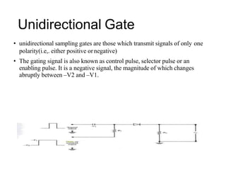
  • 4. Unidirectional Gate ? unidirectional sampling gates are those which transmit signals of only one polarity(i.e,. either positive ornegative) ? The gating signal is also known as control pulse, selector pulse or an enabling pulse. It is a negative signal, the magnitude of which changes abruptly between –V2 and –V1.
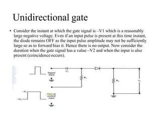
  • 5. Unidirectional gate ? Consider the instant at which the gate signal is –V1 which is a reasonably large negative voltage. Even if an input pulse is present at this time instant, the diode remains OFF as the input pulse amplitude may not be sufficiently large so as to forward bias it. Hence there is no output. Now consider the duration when the gate signal has a value –V2 and when the input is also present (coincidence occurs).
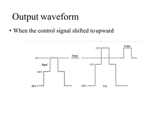
  • 6. Output waveform ? When the control signal shifted toupward
  • 7. pedestal ? When the control signal is shifted to positive value ,so it willbe superimposed on input and control signals .so the pedestal occurs
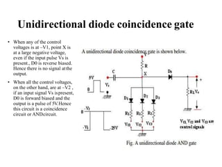
  • 8. Unidirectional diode coincidence gate ? When any of the control voltages is at –V1, point X is at a large negative voltage, even if the input pulse Vs is present., D0 is reverse biased. Hence there is no signal atthe output. ? When all the control voltages, on the other hand, are at –V2 , if an input signal Vs ispresent, D0 is forward biased and the output is a pulse of 5V .Hence this circuit is a coincidence circuit or ANDcircuit.
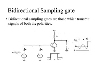
  • 9. Bidirectional Sampling gate ? Bidirectional sampling gates are those which transmit signals of both the polarities.
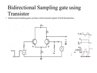
  • 10. Bidirectional Sampling gate using Transistor ? Bidirectional sampling gates are those which transmit signals of both thepolarities.
  • 11. Circuit that minimizes the pedestal ? Circuit that minimizes the pedestal
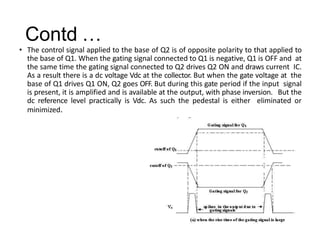
  • 12. Contd … ? The control signal applied to the base of Q2 is of opposite polarity to that applied to the base of Q1. When the gating signal connected to Q1 is negative, Q1 is OFF and at the same time the gating signal connected to Q2 drives Q2 ON and draws current IC. As a result there is a dc voltage Vdc at the collector. But when the gate voltage at the base of Q1 drives Q1 ON, Q2 goes OFF. But during this gate period if the input signal is present, it is amplified and is available at the output, with phase inversion. But the dc reference level practically is Vdc. As such the pedestal is either eliminated or minimized.
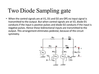
  • 13. Two Diode Sampling gate ? When the control signals are at V1, D1 and D2 are OFF,no input signal is transmitted to the output. But when control signals are at V2, diode D1 conducts if the input is positive pulses and diode D2 conducts if the input is negative pulses. Hence these bidirectional inputs are transmitted to the output. This arrangement eliminates pedestal, because of the circuit symmetry.
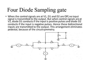
  • 14. Four Diode Sampling gate ? When the control signals are at V1, D1 and D2 are OFF,no input signal is transmitted to the output. But when control signals areat V2, diode D1 conducts if the input is positive pulses and diode D2 conducts if the input is negative pulses. Hence these bidirectional inputs are transmitted to the output. This arrangement eliminates pedestal, because of the circuitsymmetry.
  • 15. Applications ? ChopperAmplifier ? Multiplexers ? ADC ? Sampling Scope ? Sample and hold circuits
  • 16. Chopper Amplifier ? Sometimes it becomes necessary to amplify a signal v that has very small dv/dt and that the amplitude of the signal itself is very small, typically of the order of millivolts. Neither, ac amplifiers using large coupling condensers nor dc amplifiers with the associated drift would be useful for such an application. A chopper stabilized amplifier employing sampling gates canbe a useful choice in such a applications
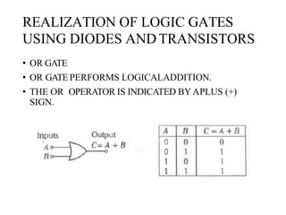
  • 17. REALIZATION OF LOGIC GATES USING DIODES AND TRANSISTORS ? OR GATE ? OR GATEPERFORMS LOGICALADDITION. ? THE OR OPERATOR IS INDICATED BYAPLUS (+) SIGN.
  • 18. OR GATE USING DIODES OPERATION: ?ASSUME THE INPUTVOLTAGES ARE EITHER 0V (LOW) OR 5V (HIGH). BOTHAAND BARE LOW: ?THE DIODES ARE OFF AND WE CAN REPLACE THE
  • 19. Contd. AIS LOWAND B ISHIGH: ? WHENAIS LOWTHE CORRESPONDING DIODE WILLBE OFFAND, B IS HIGH SO THE DIODE CORRESPONDS TO THE INPUT B WILL BE ON. ? NOW WE CAN REPLACE THE ON DIODE BY THE SHORTCIRCUIT EQUIVALENTAND THE OUTPUTC=5V. ? B IS LOWANDAIS HIGH: ? WHEN B IS LOW THE CORRESPONDING DIODE WILL BE OFFAND, A IS HIGH SO THE DIODE CORRESPONDS TO THE INPUT A WILL BE ON. ? NOW WE CAN REPLACE THE ON DIODE BY THE SHORTCIRCUIT EQUIVALENTAND THE OUTPUTC=5V. ? BOTHAAND BARE HIGH: ? WHEN BOTH THE INPUTSARE HIGH BOTH THE DIODES WILLBE ON AND THE OUTPUTC=5V.
  • 20. AND Gate ? THE AND GATEPERFORMSLOGICAL MULTIPLICATION. ? THE AND OPERATOR IS INDICATED BY USINGADOT (.) SIGN OR BY NOT SHOWING ANY OPERATOR SYMBOLATALL.
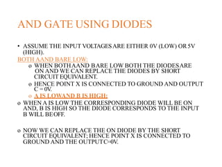
  • 21. AND GATE USING DIODES ? ASSUME THE INPUT VOLTAGESARE EITHER 0V (LOW) OR5V (HIGH). BOTH AAND BARE LOW: o WHEN BOTHAAND BARE LOW BOTH THE DIODESARE ON AND WE CAN REPLACE THE DIODES BY SHORT CIRCUIT EQUIVALENT. o HENCE POINT X IS CONNECTED TO GROUND AND OUTPUT C = 0V. o A IS LOWAND B IS HIGH: o WHEN A IS LOW THE CORRESPONDING DIODE WILL BE ON AND, B IS HIGH SO THE DIODE CORRESPONDS TO THE INPUT B WILL BEOFF. o NOW WE CAN REPLACE THE ON DIODE BY THE SHORT CIRCUIT EQUIVALENT; HENCE POINT X IS CONNECTED TO GROUND AND THE OUTPUTC=0V.
  • 22. Contd. B IS LOWANDAIS HIGH: o WHEN B IS LOW THE CORRESPONDING DIODE WILL BE ON AND, A IS HIGH SO THE DIODE CORRESPONDS TO THE INPUT AWILL BEOFF. o NOW WE CAN REPLACE THE ON DIODE BY THE SHORT CIRCUIT EQUIVALENT; HENCE POINT X IS CONNECTED TO GROUND AND THE OUTPUT C=0V. BOTHAAND BARE HIGH: o BOTH THE DIODES WILLBE OFFAND THE OUTPUTC=5V.
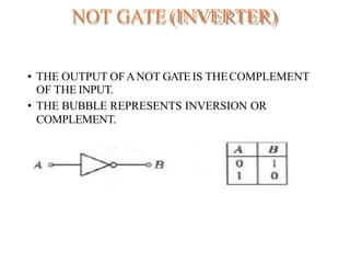
  • 23. NOT GATE(INVERTER) ? THE OUTPUT OFANOT GATEIS THECOMPLEMENT OF THE INPUT. ? THE BUBBLE REPRESENTS INVERSION OR COMPLEMENT.
  • 24. REALIZATION OF NOT GATE USING TRANSISTOR A ISHIGH: o When +5v is applied to a, the transistor will be fully on. o So maximum collector current will flow and vcc =icr, making vc or voltage at point b as zero. [Recall ce loop kvl: vc=vcc-icr]. o A IS LOW: When 0v is applied to a, the transistor will be cut-off. So ic=0ma and vc or voltage at point b is equal to vcc.
  • 25. Logic Families Vocabulary TTL (Transistor Transistor Logic) Integrated-circuit technology thatuses the bipolar transistor as the principal circuitelement. CMOS (Complimentary Metal Oxide Semiconductor) Integrated-circuit technology that uses the field-effect transistor as the principal circuit element. ECL (Emitter Coupled Logic) Integrated-circuit technology that uses the bipolar transistors configured as a differential amplifier. This eliminates saturation and improves speed but uses more power than other families.
  • 26. OTHER DIGITAL IC SPECIFICATIONS ? Drive Capabilities- sometimes referred to as fan-in or fan-out. ? Fan out- number of inputs of a logic family that can be driven by a single output. The drive capability of outputs. ? Fan in- the load an input places on an output. ? Propagation delay- has to do with the “speed” of the logic element. Lower propagation delays mean higher speed which is a desirable characteristic. ? Power Dissipation- generally, as propagation delays decrease, power consumption and heat generation increase. CMOS is noted for low power consumption.
  • 27. Fanout: the maximum number of logic inputs (of thesame logic family) that an output can drivereliably Logic families: fanout I DC fanout = min( OH , ) IIH IIL IOL 147
  • 28. Logic families: propagation delay TPD,HL TPD,LH TPD,HL – input-to-output propagation delay from HI to LO output TPD,LH – input-to-output propagation delay from LO to HIoutput Speed-power product: TPD ? Pavg 148
  • 29. Logic families: noise margin VNH VNL HI state noise margin: VNH = VOH(min) –VIH(min) LO state noise margin: VNL = VIL(max) – VOL(max) Noise margin: VN = min(VNH,VNL) 149
  • 30. TOTEM POLE NAND GATE ? First introduced by in 1964 (Texas Instruments) ? TTL has shaped digital technology in many ways ? Standard TTLfamily (e.g. 7400) is obsolete ? Newer TTLfamilies still used (e.g. 74ALS00)
  • 31. Open collector gate ? An open collector is a common type of output found on many integrated circuits(IC). ? Instead of outputting a signal of a specific voltage or current, the output signal is applied to the base of an internal NPN transistor whose collector is externalized (open) on a pin of the IC. The emitter of the transistor is connected internally to the ground pin. If the output device is a MOSFET the output is called open drain and it functions in a similar way.
  • 32. Tristate TTL ? Tristate means a state of logic other than ?1?and ?0? in which there is a high impedance state and there is no isource or isink at the output stage transistor (or MOSFET). A gate capable of being in ?1?,?0?and tristate is known as tristategate
  • 33. Direct-coupled transistor logic (DCTL) ? Direct-coupled transistor logic (DCTL) is similar to resistor– transistor logic (RTL) but the input transistor bases are connected directly to the collector outputs without any base resistors. Consequently, DCTL gates have fewer components, are more economical, and are simpler to fabricate onto integrated circuits than RTL gates. Unfortunately, DCTL has much smaller signal levels, has more susceptibility to ground noise, and requires matched transistor characteristics. The transistors are also heavily overdriven; that is a good feature in that it reduces the saturation voltage of the output transistors, but it also slows the circuit down due to a high stored charge in the base.[1] Gate fan-out is limited due to "current hogging": if the transistor base-emitter voltages (VBE) are not well matched, then the base-emitter junction of one transistor may conduct most of the input drive current at such a low base-emitter voltage that other input transistors fail to turn on
  • 34. ECL Emitter-Coupled Logic (ECL) ?PROS: Fastest logic family available(~1ns) ? CONS: low noise margin and high power dissipation ?Operated in emitter coupled geometry (recall differential amplifier or emitter-follower), transistors are biased and operate near their Q-point (nevernear saturation!) ? Logic levels. “0”: –1.7V. “1”: –0.8V ? Such strange logic levels require extra effort when interfacing to TTL/CMOS logicfamilies. ? Open LTspice example: ECLinverter… 154
  • 36. LOGIC FAMILIESAND INTRODUCTION ? WE HVE SEEN THATDIFFERENT DEVICES USE DIFFERENT VOLTAGES RANGES FOR THEIR LOGIC LEVELS. ? THEY ALSO DIFFER IN OTHER CHARACTERISTICE ? IN ORDER TOASSURE CORRECT OPERATIONWHEN GATESARE INTERCONNECTED THEY ARE NORMALLYPRODUCED IN LOGIC FAMILIES ? THE MOSTLYWIDELYUSED FAMILIESARE – COMPLEMENTARY METAL OXIDE(CMOS) – TRANSISTOR- TRANSISTOR LOGIC (TTL) – EMITTER COUPLED LOGIG (ECL)
  • 37. COPARISON OF LOGIC FAMILIES