Final_Poster-8
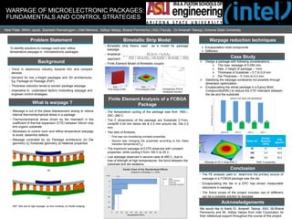
- 1. ï Design a package with following considerations : ï The max. warpage of 0.050 mm. ï Max. Z height of package â 1mm ï Thickness of Substrate â 0.7 to 0.9 mm ï Die Thickness â 0.1mm to 0.3 mm ï Satisfying the warpage constraints not possible through dimension optimization. ï Encapsulating the whole package in a Epoxy Mold Compounds(EMC) to reduce the CTE mismatch between the die and the substrate. WARPAGE OF MICROELECTRONIC PACKAGES: FUNDAMENTALS AND CONTROL STRATEGIES Neel Patel, Nithin Jacob, Seshadri Ramalingam | Intel Mentors : Aditya Vaidya, Bharat Penmecha | ASU Faculty : Dr.Amaneh Tasooji | Arizona State University Problem Statement To identify solutions to manage room and reflow temperature warpage in microelectronic packages. Background What is warpage ? Bimetallic Strip Model Finite Element Analysis of a FCBGA Package Warpage reduction techniques Conclusion ï The FE analysis used to determine the primary source of warpage in a FCBGA package was the die. ï Encapsulating the die in a EPC has shown measurable reductions in warpage. ï The future scope of the project includes use of stiffeners can be a possible solution to warpage ï Trend in electronics industry towards thin and compact devices ï Demand for low z-height packages and 3D architectures, Eg. Package on Package (PoP) ï Thickness reduction tends to worsen package warpage ï Imperative to understand factors modulating warpage and engineer control strategies ï Warpage is out of the plane displacement arising to relieve internal thermomechanical stress in a package ï Thermomechanical stress driven by the mismatch in the coefficient of thermal expansion (CTE) between Silicon chip and organic substrate ï Necessary to control room and reflow temperature warpage to avoid assembly defects ï Warpage controlled by (a) Package architecture (b) Die geometry (c) Substrate geometry (d) Material properties ï Bimetallic strip theory used as a model for package warpage. ï Analytical : approach ï Finite Element Model of Bimetallic coupon FEA Setup of BS FEA analysis of BS Comparison FEA & Analytical Solution ï The temperature cycling of the package was from 165C-- 25C--260 C. ï The Z dimensions of the package are Substrate 0.7mm, Underfill 0.04 mm below die & 0.3 mm around die, Die 0.3 mm. ï Two sets of Analysis, ï First was not considering constant properties ï Second was changing the properties according to the Glass transition temperature(Tg). ï The maximum warpage of 0.075 observed with constant properties while cooling it from 165 C to 25 C. ï Low warpage observed in second case at 260 C, due to loss of strength at high temperatures the bond between the substrate and die weakens. Temp. (C) Youngâs Modulus (GPa) CTE (ppm/C) 25 27 18.8 165 3.4 42.5 260 0.6 42.2 EMC C propertiesWarpage at 25 C using EMC C Acknowledgements We would like to thank Dr. Amaneh Tasooji, ASU; Mr.Bharat Penmecha and Mr. Aditya Vaidya from Intel Corporation for their intellectual support throughout the course of this project. SMT fails due to high warpage. (a) Non contacts, (b) Solder bridging. (a) (b) ï Encapsulation mold compounds ï Stiffeners Case Study
