


fundamentos laboratorio
- 1. Facultad de Ingenier├Ła Electr├│nica y El├®ctrica - FIEEUNMSM Circuitos Digitales Fundamentos Prof. Ing. Oscar Casimiro F.I.E.E Sem. 2011-I
- 2. Facultad de Ingenier├Ła Electr├│nica y El├®ctrica - FIEEUNMSM Most natural quantities that we see are analog and vary continuously. Analog systems can generally handle higher power than digital systems. SummarySummarySummary Digital systems can process, store, and transmit data more efficiently but can only assign discrete values to each point. Analog Quantities 1 100 A .M. 95 90 85 80 75 2 3 4 5 6 7 8 9 10 11 12 1 2 3 4 5 6 7 8 9 10 11 12 P.M. Temperature (┬░F) 70 Time of day
- 3. Facultad de Ingenier├Ła Electr├│nica y El├®ctrica - FIEEUNMSM Many systems use a mix of analog and digital electronics to take advantage of each technology. A typical CD player accepts digital data from the CD drive and converts it to an analog signal for amplification. SummarySummarySummary Analog and Digital Systems Digital data CD drive 10110011101 Analog reproduction of music audio signal Speaker Sound waves Digital-to-analog converter Linear amplifier
- 4. Facultad de Ingenier├Ła Electr├│nica y El├®ctrica - FIEEUNMSM Digital electronics uses circuits that have two states, which are represented by two different voltage levels called HIGH and LOW. The voltages represent numbers in the binary system. SummarySummarySummary Binary Digits and Logic Levels In binary, a single number is called a bit (for binary digit). A bit can have the value of either a 0 or a 1, depending on if the voltage is HIGH or LOW. HIGH LOW VH(max) VH(min) VL(max) VL(min) Invalid
- 5. Facultad de Ingenier├Ła Electr├│nica y El├®ctrica - FIEEUNMSM Digital waveforms change between the LOW and HIGH levels. A positive going pulse is one that goes from a normally LOW logic level to a HIGH level and then back again. Digital waveforms are made up of a series of pulses. SummarySummarySummary Digital Waveforms Falling or leading edge (b) NegativeŌĆōgoing pulse HIGH Rising or trailing edge LOW (a) PositiveŌĆōgoing pulse HIGH Rising or leading edge Falling or trailing edge LOW t0 t1 t0 t1
- 6. Facultad de Ingenier├Ła Electr├│nica y El├®ctrica - FIEEUNMSM Actual pulses are not ideal but are described by the rise time, fall time, amplitude, and other characteristics. SummarySummarySummary Pulse Definitions 90% 50% 10% Base line Pulse width Rise time Fall time Amplitude tW tr tf Undershoot Ringing Overshoot Ringing Droop
- 7. Facultad de Ingenier├Ła Electr├│nica y El├®ctrica - FIEEUNMSM Periodic pulse waveforms are composed of pulses that repeats in a fixed interval called the period. The frequency is the rate it repeats and is measured in hertz. SummarySummarySummary Periodic Pulse Waveforms T f 1 = f T 1 = The clock is a basic timing signal that is an example of a periodic wave. What is the period of a repetitive wave if f = 3.2 GHz? === GHz2.3 11 f T 313 ps
- 8. Facultad de Ingenier├Ła Electr├│nica y El├®ctrica - FIEEUNMSM SummarySummarySummary Pulse Definitions In addition to frequency and period, repetitive pulse waveforms are described by the amplitude (A), pulse width (tW) and duty cycle. Duty cycle is the ratio of tW to T. Volts Time Amplitude (A) Pulse width (tW) Period, T
- 9. Facultad de Ingenier├Ła Electr├│nica y El├®ctrica - FIEEUNMSM A timing diagram is used to show the relationship between two or more digital waveforms, SummarySummarySummary Timing Diagrams Clock A B C A diagram like this can be observed directly on a logic analyzer.
- 10. Facultad de Ingenier├Ła Electr├│nica y El├®ctrica - FIEEUNMSM Data can be transmitted by either serial transfer or parallel transfer. SummarySummarySummary Serial and Parallel Data Computer Modem 1 0 1 1 0 0 1 0 t0 t1 t2 t3 t4 t5 t6 t7 Computer Printer 0 t0 t1 1 0 0 1 1 0 1
- 11. Facultad de Ingenier├Ła Electr├│nica y El├®ctrica - FIEEUNMSM SummarySummarySummary Basic Logic Functions True only if all input conditions are true. True only if one or more input conditions are true. Indicates the opposite condition.
- 12. Facultad de Ingenier├Ła Electr├│nica y El├®ctrica - FIEEUNMSM SummarySummarySummary Basic System Functions And, or, and not elements can be combined to form various logic functions. A few examples are: The comparison function Basic arithmetic functions Adder Two binary numbers Carry out A B Cout CinCarry in Sum╬Ż Two binary numbers Outputs A B A< B A= B A> B Comparator
- 13. Facultad de Ingenier├Ła Electr├│nica y El├®ctrica - FIEEUNMSM SummarySummarySummary Basic System Functions The encoding function The decoding function Decoder Binary input 7-segment display Encoder9 8 9 4 5 6 1 2 3 0 . +/ŌĆō 7 Calculator keypad 8 7 6 5 4 3 2 1 0 HIGH Binary code for 9 used for storage and/or computation
- 14. Facultad de Ingenier├Ła Electr├│nica y El├®ctrica - FIEEUNMSM SummarySummarySummary Basic System Functions The data selection function Multiplexer A Switching sequence control input B C Ōłåt2 Ōłåt3 Ōłåt1 Ōłåt2 Ōłåt3 Ōłåt1 Demultiplexer D E F Data from Ato D Data from Bto E Data from Cto F Data from Ato D Ōłåt1 Ōłåt2 Ōłåt3 Ōłåt1 Switching sequence control input
- 15. Facultad de Ingenier├Ła Electr├│nica y El├®ctrica - FIEEUNMSM SummarySummarySummary Basic System Functions The counting function ŌĆ”and other functions such as code conversion and storage. Input pulses 1 Counter Parallel output lines Binary code for 1 Binary code for 2 Binary code for 3 Binary code for 4 Binary code for 5 Sequence of binary codes that represent the number of input pulses counted. 2 3 4 5
- 16. Facultad de Ingenier├Ła Electr├│nica y El├®ctrica - FIEEUNMSM SummarySummarySummary Basic System Functions One type of storage function is the shift register, that moves and stores data each time it is clocked. 0 0 0 00101 Initially,the register contains onlyinvalid data or all zeros as shown here. 1 0 0 0010 First bit (1) is shifted serially into the register. 0 1 0 001 Second bit (0) is shifted serially into register and first bit is shifted right. 1 0 1 00 Third bit (1) is shifted into register and the first and second bits are shifted right. 0 1 0 1 Fourth bit (0) is shifted into register and the first,second,and third bits are shifted right.The register now stores all four bits and is full. Serial bits on input line
- 17. Facultad de Ingenier├Ła Electr├│nica y El├®ctrica - FIEEUNMSM SummarySummarySummary Integrated Circuits Plastic case Pins Chip Cutaway view of DIP (Dual-In-line Pins) chip: The TTL series, available as DIPs are popular for laboratory experiments with logic.
- 18. Facultad de Ingenier├Ła Electr├│nica y El├®ctrica - FIEEUNMSM SummarySummarySummary An example of laboratory prototyping is shown. The circuit is wired using DIP chips and tested. Integrated Circuits In this case, testing can be done by a computer connected to the system. DIP chips
- 19. Facultad de Ingenier├Ła Electr├│nica y El├®ctrica - FIEEUNMSM SummarySummarySummary Integrated Circuits DIP chips and surface mount chips Pin 1 Dual in-line package Small outline IC (SOIC)
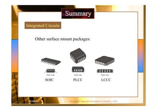
- 20. Facultad de Ingenier├Ła Electr├│nica y El├®ctrica - FIEEUNMSM SummarySummarySummary Integrated Circuits Other surface mount packages: SOIC PLCC LCCC End viewEnd viewEnd view
- 21. Facultad de Ingenier├Ła Electr├│nica y El├®ctrica - FIEEUNMSM SummarySummarySummary Test and Measurement Instruments HORIZONTALVERTICAL TRIGGER 5 s 5 ns POSITION CH 1 CH 2 EXT TRIG AC-DC-GND 5V 2 mV VOLTS/DIV COUPLING CH 1 CH 2 BOTH POSITION AC-DC-GND 5V 2 mV VOLTS/DIV COUPLING SEC/DIV POSITION SLOPE ├É + LEVEL SOURCE CH1 CH2 EXT LINE TRIG COUP DC AC DISPLAY INTENSITY PROBECOMP 5V The front panel controls for a general-purpose oscilloscope can be divided into four major groups.
- 22. Facultad de Ingenier├Ła Electr├│nica y El├®ctrica - FIEEUNMSM SummarySummarySummary Test and Measurement Instruments Ch 1 External trigger Conversion/storage (Digital scopes only) Signal coupling AC DC GND Amp Ch 2 Conversion/storage (Digital scopes only) AC DC GND Amp Volts/Div Vertical position AC DC Ext Trigger source External trigger coupling Ch 1 Ch 2 Line Trigger circuits Trigger level and slope Time base Sec/Div Horizontal position Control and process (Digital scopes only) Intensity AC DC to all sections Power supply Vertical section Display section Horizontal sectionTrigger section Digital only Analog only For measuring digital signals, use DC coupling Normally, trigger on the slower of two waveforms when comparing signals. ┬® 2009 Pearson Education
- 23. Facultad de Ingenier├Ła Electr├│nica y El├®ctrica - FIEEUNMSM SummarySummarySummary Test and Measurement Instruments The logic analyzer can display multiple channels of digital information or show data in tabular form.
- 24. Facultad de Ingenier├Ła Electr├│nica y El├®ctrica - FIEEUNMSM SummarySummarySummary Test and Measurement Instruments V 1 s 1 s 40 mA 10 A COM Range Autorange Touch/Hold Fused OFF V V Hz mV A 0.01 V The DMM can make three basic electrical measurements. Voltage Resistance Current In digital work, DMMs are useful for checking power supply voltages, verifying resistors, testing continuity, and occasionally making other measurements.
- 25. Facultad de Ingenier├Ła Electr├│nica y El├®ctrica - FIEEUNMSM SummarySummarySummary Programmable Logic Programmable logic devices (PLDs) are an alternative to fixed function devices. The logic can be programmed for a specific purpose. In general, they cost less and use less board space that fixed function devices. Fixed OR array and output logic Programmable AND array A PAL device is a form of PLD that uses a combination of a programmable AND array and a fixed OR array:
- 26. Glossary ŌĆō FIEE - ┬® 2010 Selected Key TermsSelected Key TermsSelected Key Terms Analog Digital Binary Bit Pulse Being continuous or having continuous values. Related to digits or discrete quantities; having a set of discrete values. Having two values or states; describes a number system that has a base of two and utilizes 1 and 0 as its digits. A binary digit, which can be a 1 or a 0. A sudden change from one level to another, followed after a time, called the pulse width, by a sudden change back to the original level.
- 27. Glossary ŌĆō FIEE - ┬® 2010 Selected Key TermsSelected Key TermsSelected Key Terms Clock Gate NOT AND OR A basic timing signal in a digital system; a periodic waveform used to synchronize actions. A logic circuit that performs a basic logic operations such as AND or OR. A basic logic function that performs inversion. A basic logic operation in which a true (HIGH) output occurs only when all input conditions are true (HIGH). A basic logic operation in which a true (HIGH) output occurs when when one or more of the input conditions are true (HIGH).
- 28. Glossary ŌĆō FIEE - ┬® 2010 Selected Key TermsSelected Key TermsSelected Key Terms Fixed-function logic Programmable logic A category of digital integrated circuits having functions that cannot be altered. A category of digital integrated circuits capable of being programmed to perform specified functions.