Heterointegration Coming of Age in 2015 - MEF 2015

Heterogeneous integration, which involves integrating different device technologies such as CMOS and MEMS onto a single chip, is coming of age commercially. This integration allows for more sophisticated capabilities in smaller form factors by enabling multiple sensors, signal processing, and telemetry capabilities. Commercial examples of heterogeneous integration discussed in the document include Sony's stacked CMOS image sensors using TSVs, SiTime's MEMS oscillators integrated using epi-poly sealing, and various MEMS startups developing novel integration approaches like mCube's monolithic MEMS-on-CMOS using through-silicon vias. The document examines the definition and various approaches to heterogeneous integration in the microelectronics industry.
![15-IN-15: ANALOG,MEMS AND SENSOR STARTUPS TO WATCHIN
2015
“Here are fifteen startups that are eager
to change the world of electronics and
that we think are worth keeping an eye on
in 2015 if you are interested in analog,
MEMS and sensors.”
[Peter Clarke in EETimes, 02 January 2015.]](https://image.slidesharecdn.com/633b8fd8-918c-444c-98b8-2f42b8b4eb9b-150427090731-conversion-gate02/85/Heterointegration-Coming-of-Age-in-2015-MEF-2015-5-320.jpg)
![HETEROINTEGRATION SPOOR IN MEMS AND SENSOR START-UPS
Definition of SPOOR
1: a track, a trail, a scent, or droppings
especially of a wild animal
2: a trace by which the progress of
someone or something may be followed
What would we find, I thought to myself, were
we to look for heterointegration spoor
amongst these 15 notable start-ups?
[3D+, 23 February 2015]](https://image.slidesharecdn.com/633b8fd8-918c-444c-98b8-2f42b8b4eb9b-150427090731-conversion-gate02/85/Heterointegration-Coming-of-Age-in-2015-MEF-2015-6-320.jpg)
![HOW IS HETEROGENEOUS 3D INTEGRATION DEFINED?
“There are certainly different understandings in the microelectronics
community regarding the definition of heterogeneous 3D integration.”
1) Integration of different devices such as a CMOS processor
and a memory
2) Integration of different substrate materials necessary for the
condition (e.g. GaAs / silicon)
3) Integration of components with significant different device
technologies as e.g. CMOS and MEMS
[Peter Ramm, PhD, Fraunhofer EMFT, in 3D InCites, 16 January 2015]](https://image.slidesharecdn.com/633b8fd8-918c-444c-98b8-2f42b8b4eb9b-150427090731-conversion-gate02/85/Heterointegration-Coming-of-Age-in-2015-MEF-2015-10-320.jpg)
![HETEROINTEGRATION: CMOS IMAGE SENSORS
IFTLE 172 Sony TSV Stacked CMOS Image Sensors Finally Arrive in 2013
“Many of us can recall 2008 when Toshiba commercialized the first CMOS image
sensor with TSV last /backside. We called these the first 3DIC products, when in
reality they were only 1 layer devices.
The Sony ISX014 8MP sensor features 1.12um pixels and integrated high speed ISP.
The pixel layer and logic layer part are manufactured as separate chips and stacked
by using TSVs. Previously the pixel and logic circuit of Sony’s back side illuminated
(BSI) CMOS image sensor were formed during the same fabrication process.”
[Phil Garrou, PhD, Solid State Technology, 09 December 2013]
Q4 2014 iPhone 6 sales 75M Units](https://image.slidesharecdn.com/633b8fd8-918c-444c-98b8-2f42b8b4eb9b-150427090731-conversion-gate02/85/Heterointegration-Coming-of-Age-in-2015-MEF-2015-12-320.jpg)
![HETEROINTEGRATION: INVISAGE
About InVisage:
“Harnessing the power of custom—designed
nanoscale materials, InVisage has created a new
generation of QuantumFilm™ based image
sensors that puts the camera in a whole new
light.”
“QuantumFilm was designed to absorb 100% of
the light we see with our own eyes and do so in a
film whose thickness is measured in
nanometers. We took the magic of photographic
film … and integrated it intimately onto a silicon
chip.” Target markets: mobile devices such as
camera phones and digital cameras.
About the Market:
1.3B smartphone shipments CY2014
100M digital camera shipments CY2012
86M global automotive sales CY2014
About InVisage and Heterointegration:
QuantumFilm is “made from materials similar to
conventional film—a polymer with embedded
particles—instead of silver grains like photographic
film the embedded particles are quantum dots.”
The QuantumFilm is painted “… atop a low-cost
wafer that has the electrode array for super-dense
high-pixel-count images, but without any of the
expensive CMOS photodetectors that make up the
bulk of conventional digital camera sensors.”
[R. Colin Johnson, EETimes, 22 March 2010]
InVisage QuantumFilm](https://image.slidesharecdn.com/633b8fd8-918c-444c-98b8-2f42b8b4eb9b-150427090731-conversion-gate02/85/Heterointegration-Coming-of-Age-in-2015-MEF-2015-15-320.jpg)
Heterointegration Coming of Age in 2015 - MEF 2015
- 1. HETEROGENEOUS INTEGRATION: COMING OF AGE IN 2015 Paul Werbaneth Contributing Editor, 3D InCites / 3D+ and Alissa Fitzgerald, PhD Managing Member, A.M. Fitzgerald & Associates
- 2. OUTLINE • About 3D InCites / 3D+ / A.M. Fitzgerald & Associates • “15-in15: Analog, MEMS and Sensors Startups to Watch in 2015” • Why Integration? • How Is 3D Heterogeneous Integration Defined? • Commercial Heterointegration: Coming of Age • Heterointegration Risks and Challenges • Conclusion
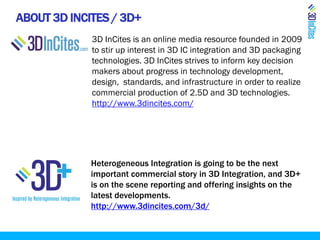
- 3. ABOUT 3D INCITES / 3D+ 3D InCites is an online media resource founded in 2009 to stir up interest in 3D IC integration and 3D packaging technologies. 3D InCites strives to inform key decision makers about progress in technology development, design, standards, and infrastructure in order to realize commercial production of 2.5D and 3D technologies. http://www.3dincites.com/ Heterogeneous Integration is going to be the next important commercial story in 3D Integration, and 3D+ is on the scene reporting and offering insights on the latest developments. http://www.3dincites.com/3d/
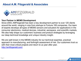
- 4. About A.M. Fitzgerald & Associates © AMFitzgerald 2015 Page 4 Your Partner in MEMS Development Since 2003, AMFitzgerald has been a key development partner to over 125 clients around the world, ranging in size from startups to Fortune 100 companies. Our team of experts develops all types of MEMS sensors and actuators for applications in the consumer electronics, medical devices, industrial, aerospace, and scientific markets. We also help shape our customers' business and product strategies by leveraging our deep technical knowledge and unique industry insight. We are well known in the MEMS industry for our technical expertise, practical approach to manufacturing, and forthright assessment of risk. Our customers trust us with their most critical projects and return to us year after year. http://amfitzgerald.com/
- 5. 15-IN-15: ANALOG,MEMS AND SENSOR STARTUPS TO WATCHIN 2015 “Here are fifteen startups that are eager to change the world of electronics and that we think are worth keeping an eye on in 2015 if you are interested in analog, MEMS and sensors.” [Peter Clarke in EETimes, 02 January 2015.]
- 6. HETEROINTEGRATION SPOOR IN MEMS AND SENSOR START-UPS Definition of SPOOR 1: a track, a trail, a scent, or droppings especially of a wild animal 2: a trace by which the progress of someone or something may be followed What would we find, I thought to myself, were we to look for heterointegration spoor amongst these 15 notable start-ups? [3D+, 23 February 2015]
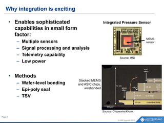
- 7. © AMFitzgerald 2015 Page 7 • Enables sophisticated capabilities in small form factor: – Multiple sensors – Signal processing and analysis – Telemetry capability – Low power • Methods – Wafer-level bonding – Epi-poly seal – TSV Why integration is exciting Integrated Pressure Sensor Source: IMD MEMS sensor Stacked MEMS and ASIC chips, wirebonded Source: Chipworks/Kionix
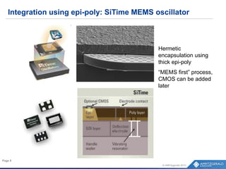
- 8. © AMFitzgerald 2015 Page 8 Integration using epi-poly: SiTime MEMS oscillator Hermetic encapsulation using thick epi-poly “MEMS first” process, CMOS can be added later
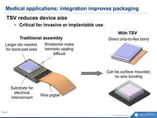
- 9. Medical applications: integration improves packaging © AMFitzgerald 2015 Page 9 Larger die needed for bond pad area Substrate for electrical interconnect Wirebonds make hermetic sealing difficult Wire pigtail Direct chip-to-flex bond Can be surface mounted, no wire bonding With TSV Traditional assembly TSV reduces device size • Critical for invasive or implantable use
- 10. HOW IS HETEROGENEOUS 3D INTEGRATION DEFINED? “There are certainly different understandings in the microelectronics community regarding the definition of heterogeneous 3D integration.” 1) Integration of different devices such as a CMOS processor and a memory 2) Integration of different substrate materials necessary for the condition (e.g. GaAs / silicon) 3) Integration of components with significant different device technologies as e.g. CMOS and MEMS [Peter Ramm, PhD, Fraunhofer EMFT, in 3D InCites, 16 January 2015]
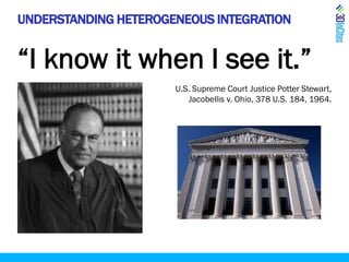
- 11. UNDERSTANDING HETEROGENEOUS INTEGRATION “I know it when I see it.” U.S. Supreme Court Justice Potter Stewart, Jacobellis v. Ohio, 378 U.S. 184, 1964.
- 12. HETEROINTEGRATION: CMOS IMAGE SENSORS IFTLE 172 Sony TSV Stacked CMOS Image Sensors Finally Arrive in 2013 “Many of us can recall 2008 when Toshiba commercialized the first CMOS image sensor with TSV last /backside. We called these the first 3DIC products, when in reality they were only 1 layer devices. The Sony ISX014 8MP sensor features 1.12um pixels and integrated high speed ISP. The pixel layer and logic layer part are manufactured as separate chips and stacked by using TSVs. Previously the pixel and logic circuit of Sony’s back side illuminated (BSI) CMOS image sensor were formed during the same fabrication process.” [Phil Garrou, PhD, Solid State Technology, 09 December 2013] Q4 2014 iPhone 6 sales 75M Units
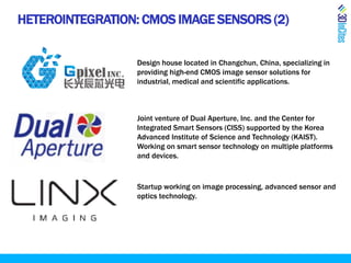
- 13. HETEROINTEGRATION: CMOS IMAGE SENSORS (2) Joint venture of Dual Aperture, Inc. and the Center for Integrated Smart Sensors (CISS) supported by the Korea Advanced Institute of Science and Technology (KAIST). Working on smart sensor technology on multiple platforms and devices. Design house located in Changchun, China, specializing in providing high-end CMOS image sensor solutions for industrial, medical and scientific applications. Startup working on image processing, advanced sensor and optics technology.
- 14. HETEROINTEGRATION: CAMBRIDGE CMOS SENSORS About CCS: Industry leader in advanced sensor solutions and sensor technology for monitoring indoor air quality (IAQ), including VOCs and hazardous gases (such as CO), outdoor air pollution levels, and breath analysis. CCS is a fabless semiconductor company; the sensors themselves are fabricated on a standard CMOS MEMS process. The CCS family of MOX gas sensors enable ultra- low power consumption (<10mW) for gas sensing, which means the CSS sensors can find practical use in battery operated portable devices such as smartphones and wearables. About the Market: >7.2B human beings March 2015 >1.4B households worldwide 1.3B smartphone shipments CY2014 86M global automotive sales CY2014 About CCS and Heterointegration: CSS is a member of the MSP Project - Multi Sensor Platform for Smart Building Management. The MSP Project “… is focused on the development of highly innovative components and sensors based on Key Enabling Technologies (KETs). The MSP- project employs Through-Silicon-Via (TSV) technology for 3D-integration of these devices on CMOS electronic platform chips to innovative smart systems capable for indoor and outdoor environmental monitoring.” CCS Micro-Hotplate
- 15. HETEROINTEGRATION: INVISAGE About InVisage: “Harnessing the power of custom—designed nanoscale materials, InVisage has created a new generation of QuantumFilm™ based image sensors that puts the camera in a whole new light.” “QuantumFilm was designed to absorb 100% of the light we see with our own eyes and do so in a film whose thickness is measured in nanometers. We took the magic of photographic film … and integrated it intimately onto a silicon chip.” Target markets: mobile devices such as camera phones and digital cameras. About the Market: 1.3B smartphone shipments CY2014 100M digital camera shipments CY2012 86M global automotive sales CY2014 About InVisage and Heterointegration: QuantumFilm is “made from materials similar to conventional film—a polymer with embedded particles—instead of silver grains like photographic film the embedded particles are quantum dots.” The QuantumFilm is painted “… atop a low-cost wafer that has the electrode array for super-dense high-pixel-count images, but without any of the expensive CMOS photodetectors that make up the bulk of conventional digital camera sensors.” [R. Colin Johnson, EETimes, 22 March 2010] InVisage QuantumFilm
- 16. HETEROINTEGRATION: ISORG About ISORG: ISORG converts plastic and glass surfaces into smart surfaces,” offering “a new generation of high performance opto-electronic sensors with 3D product integration capability recognizing any shapes and form factors.” Target markets include medical equipment; health care and life sciences; industry 4.0 and Internet-Of-Things; consumer electronics; home appliances; smart building and lighting; safety and security; environment; and toys and education. About the Market: >40B lamp sockets in CY2014 >10B annual bulb shipments CY2015 6.9B RFID Tags sold CY2014 About ISORG and Heterointegration: The ISORG process is “compatible with system-on- foil integration (co-integration of printed sensors with discrete components and integrated circuits on plastic).” Current manufacturing is being done on the ISORG pilot manufacturing line, Grenoble, on 32cm x 38cm plastic foils; a mass production demonstrator is planned for 2015-end, on 60cm x 70cm plastic foils. ISORG Large Area Image Sensor
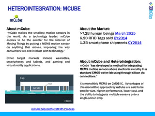
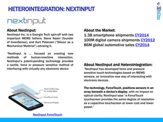
- 17. HETEROINTEGRATION: MCUBE About mCube: “mCube makes the smallest motion sensors in the world. As a technology leader, mCube aspires to be the enabler for the Internet of Moving Things by putting a MEMS motion sensor on anything that moves, improving the way consumers live and interact with technology.” Other target markets include wearables, smartphones and tablets, and gaming and virtual reality applications. About the Market: >7.2B human beings March 2015 6.9B RFID Tags sold CY2014 1.3B smartphone shipments CY2014 About mCube and Heterointegration: mCube “has developed a method for integrating MEMS motion sensors above electronic circuitry in a standard CMOS wafer fab using through-silicon via connections.” It’s monolithic MEMS on CMOS IC. Advantages of this monolithic approach by mCube are said to be smaller size, higher performance, lower cost, and the ability to integrate multiple sensors onto a single-silicon chip. mCube Monolithic MEMS Process
- 18. HETEROINTEGRATION: NEXTINPUT About NextInput: NextInput Inc. is a Georgia Tech spin-off with two important MEMS fathers, Steve Nasiri (founder of InvenSense), and Kurt Petersen (“Silicon as a Mechanical Material”) advising it. “NextInput is … focused on creating new methods of human-machine interaction. NextInput’s patent-pending technology provides a tactile, force or pressure sensitive method of interfacing with virtually any electronic device About the Market: 1.3B smartphone shipments CY2014 100M digital camera shipments CY2012 86M global automotive sales CY2014 About NextInput and Heterointegration: “NextInput has developed force and pressure sensitive touch technologies based on MEMS sensors, an innovative new way of interacting with electronic devices. The technology, ForceTouch, positions sensors in an array beneath a device’s display, with no impact on optical clarity; NextInput says “a ForceTouch touchscreen provides the same degree of resolution as a capacitive touchscreen at lower cost and lower power.” . NextInput ForceTouch
- 19. © AMFitzgerald 2015 Page 19 MEMS integration risks and challenges • Yield loss in wafer-level integration – Good CMOS bonded to bad MEMS  CMOS yield > 95%  MEMS yield 70-90% • Mechanical reliability problems – CTE mismatch: cracking, delamination – Stress: warping, shifted sensor offsets • For some products, package-level integration will persist until MEMS yields improve
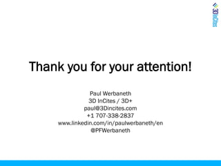
- 20. CONCLUSION: THIS TALK AS A WORD CLOUD
- 21. Thank you for your attention! Paul Werbaneth 3D InCites / 3D+ paul@3Dincites.com +1 707-338-2837 www.linkedin.com/in/paulwerbaneth/en @PFWerbaneth