J Zazzera L
- 1. Advancements For Sub 45nm Fixed Abrasive STI CMP John Gagliardi, Andrey Zagrebelny, Gagliardi Andre Zagrebeln Bill Joseph, Larry Zazzera 3M Company p y 3M NCCAVS CMP Users Group at Semicon West Moscone Center, San Francisco, CA
- 2. Outline • Background – Timeline of developments leading to Advancements for Sub 45 nm FA STI CMP – The FA Process and Outstanding Planarization • Current FA STI CMP Roadmap – 65 nm, 45 nm and Sub 45 nm • Advancements for 45 nm and sub 45 nm – Chemistry – Abrasive – CMP process and performance • Summary and Conclusion 3M NCCAVS CMP Users Group at Semicon West Moscone Center, San Francisco, CA
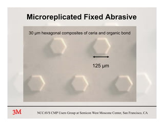
- 3. Microreplicated Fixed Abrasive 30 µm hexagonal composites of ceria and organic bond 125 µm 3M NCCAVS CMP Users Group at Semicon West Moscone Center, San Francisco, CA
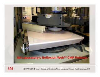
- 4. 3M Laboratory’s Reflexion Web™ CMP Polisher 3M NCCAVS CMP Users Group at Semicon West Moscone Center, San Francisco, CA
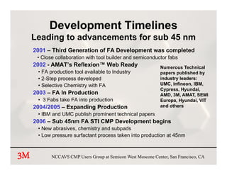
- 5. Development Timelines Leading to advancements for sub 45 nm 2001 – Third Generation of FA Development was completed • Close collaboration with tool builder and semiconductor fabs 2002 - AMAT’s Reflexion™ Web Ready Numerous Technical • FA production tool available to Industry papers published by • 2-Step process developed industry leaders: • Selective Chemistry with FA UMC, Infineon, IBM, Cypress, Hyundai, 2003 – FA In Production AMD, 3M, AMAT, SEMI • 3 Fabs take FA into production F b t k i t d ti Europa, Hyundai, VIT 2004/2005 – Expanding Production and others • IBM and UMC publish prominent technical papers 2006 – Sub 45nm FA STI CMP Development begins • New abrasives, chemistry and subpads • Low pressure surfactant process taken into production at 45nm 3M NCCAVS CMP Users Group at Semicon West Moscone Center, San Francisco, CA
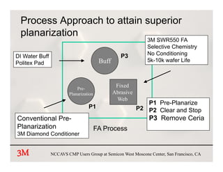
- 6. Process Approach to attain superior planarization 3M SWR550 FA Selective Chemistry DI Water Buff P3 No Conditioning Politex Pad Buff 5k-10k wafer Life Pre- Fixed Planarization Abrasive Web P1 Pre-Planarize P1 P2 P2 Clear and Stop Conventional Pre Pre- P3 Remove Ceria Planarization FA Process 3M Diamond Conditioner 3M NCCAVS CMP Users Group at Semicon West Moscone Center, San Francisco, CA
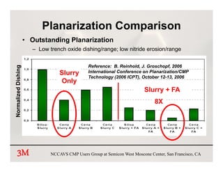
- 7. Planarization Comparison • Outstanding Planarization – Low trench oxide dishing/range; low nitride erosion/range Reference: B. Reinhold, J. Groschopf, 2006 hing Slurry y International Conference on Planarization/CMP ized Dish Technology (2006 ICPT), October 12-13, 2006 Only Slurry + FA Normali 8X 3M NCCAVS CMP Users Group at Semicon West Moscone Center, San Francisco, CA
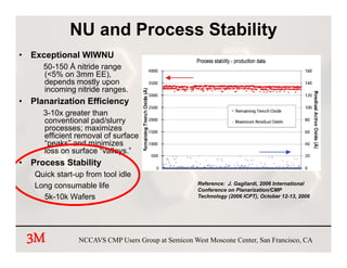
- 8. NU and Process Stability • Exceptional WIWNU 50-150 Å nitride range (<5% on 3mm EE), depends mostly upon incoming nitride ranges. • Planarization Efficiency 3-10x greater than g conventional pad/slurry processes; maximizes efficient removal of surface “peaks” and minimizes loss on surface “valleys ” valleys. • Process Stability Quick start-up from tool idle Reference: J. Gagliardi, 2006 International J Gagliardi Long consumable life Conference on Planarization/CMP 5k-10k Wafers Technology (2006 ICPT), October 12-13, 2006 3M NCCAVS CMP Users Group at Semicon West Moscone Center, San Francisco, CA
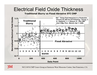
- 9. Electrical Field Oxide Thickness Traditional Slurry vs Fixed Abrasive STI CMP rical Field Oxide 1.2 Ref: “Using Fixed Abrasives in a Production Process for 200 mm STI Polishing,” Huang, C. Traditional K., Gagliardi, J. J., Gleason, E., 16th CMP Slurry User s Mtg. Proc., Munich Apr. 7, 2006, User’s Mtg Proc Munich, Apr 7 2006 1.1 1 zed Electr 0.9 Fixed Abrasive Normaliz 0.8 1 2 3 4 5 6 7 1 2 3 4 5 6 7 8 9 10 11 12 13 WAFER 0.7 0 200 400 600 800 1000 Data P i t D t Point 3M NCCAVS CMP Users Group at Semicon West Moscone Center, San Francisco, CA
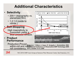
- 10. Additional Characteristics • Selectivity ~ 200:1 (topography vs. planarized film) ~ 1.2:1.0 (oxide to nitride.) • S fS Self-Stopping High insensitivity to o e po s yields overpolish y e ds a wide process window. • Product Performance Production-ProvenReference: Y. Moon, A. Kapur, R. Venigalla, L. Economikos, 2006 within-roll and roll-to- International Conference on Planarization/CMP Technology (2006 roll consistency ICPT) October 12-13, 2006 consistency. ICPT), O t b 12 13 3M NCCAVS CMP Users Group at Semicon West Moscone Center, San Francisco, CA
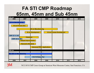
- 11. FA STI CMP Roadmap 300 mm 65nm, 65nm 45nm and Sub 45nm 2006 2007 2008 2009 2010 2011 2012 65 nm Manufacturing 45 nm Process Dev. 45 nm Manufacturing 32 nm D Development l t 32 nm P Process D Development l t SWR 521 & 542 Chemistry SWR 548 & 550 Subpad Improvements p p Nanoceria Abrasives Advanced FEOL Applications 200 mm Sub 250 nm Manufacturing R14 FA Rotary Pad 2006 2007 2008 2009 2010 2011 2012 3M NCCAVS CMP Users Group at Semicon West Moscone Center, San Francisco, CA
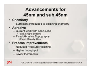
- 12. Advancements for 45nm and sub 45nm • Chemistry – Surfactant introduced to polishing chemistry • Abrasive – Current work with nano ceria nano-ceria • Size, Shape, Loading – Fixed Abrasive Topography • Shape Density, Size Shape, Density • Process Improvements – Reduced Pressure Polishing g – Higher throughput – Lower Increments 3M NCCAVS CMP Users Group at Semicon West Moscone Center, San Francisco, CA
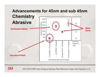
- 13. Advancements for 45nm and sub 45nm Chemistry Abrasive Surfactant Added Nano Ceria Standard Polish 3M NCCAVS CMP Users Group at Semicon West Moscone Center, San Francisco, CA
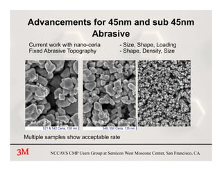
- 14. Advancements for 45nm and sub 45nm Abrasive Ab i Current work with nano-ceria - Size, Shape, Loading p g p y Fixed Abrasive Topography - Shape, Density, Size p , y, 521 & 542 Ceria, 150 nm 548, 550 Ceria, 135 nm Multiple samples show acceptable rate p p p 3M NCCAVS CMP Users Group at Semicon West Moscone Center, San Francisco, CA
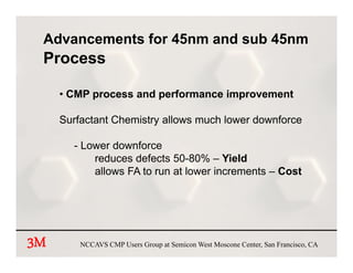
- 15. Advancements for 45nm and sub 45nm Process • CMP process and performance improvement Surfactant Chemistry allows much lower downforce - Lower downforce reduces defects 50-80% – Yield allows FA to run at lower increments – Cost 3M NCCAVS CMP Users Group at Semicon West Moscone Center, San Francisco, CA
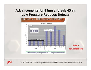
- 16. Advancements for 45nm and sub 45nm Low Pressure Reduces Defects From a KLA-Tencor SP2 KLA T 3M NCCAVS CMP Users Group at Semicon West Moscone Center, San Francisco, CA
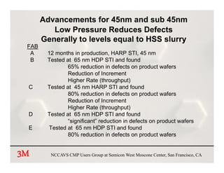
- 17. Advancements for 45nm and sub 45nm Low Pressure Reduces Defects Generally to levels equal to HSS slurry FAB A 12 months in production, HARP STI 45 nm production STI, B Tested at 65 nm HDP STI and found 65% reduction in defects on product wafers Reduction of Increment Higher Rate (throughput) C Tested at 45 nm HARP STI and found 80% reduction in defects on product wafers Reduction of Increment Higher Rate (throughput) D Tested at 65 nm HDP STI and found “significant” reduction i d f t on product wafers “ i ifi t” d ti in defects d t f E Tested at 65 nm HDP STI and found 80% reduction in defects on product wafers 3M NCCAVS CMP Users Group at Semicon West Moscone Center, San Francisco, CA
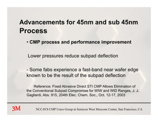
- 18. Advancements for 45nm and sub 45nm Process • CMP process and performance improvement Lower pressures reduce subpad deflection -S Some f b experience a f t b d near wafer edge fabs i fast-band f d known to be the result of the subpad deflection Reference: Fixed Abrasive Direct STI CMP Allows Elimination of the Conventional Subpad Compromise for WIW and WID Ranges, J. J. Gagliardi, Abs. 915, 204th Elec. Chem. Soc., Oct. 12-17, 2003 3M NCCAVS CMP Users Group at Semicon West Moscone Center, San Francisco, CA
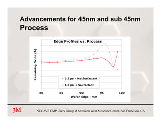
- 19. Advancements for 45nm and sub 45nm Process 4000 Edge Profiles vs. Process 3500 ning Oxide (Ă…) 3000 2500 2000 1500 Remain 1000 3.5 psi - No Surfactant 500 1.5 1 5 psi + Surfactant 0 80 85 90 95 100 Wafer Edge - mm 3M NCCAVS CMP Users Group at Semicon West Moscone Center, San Francisco, CA
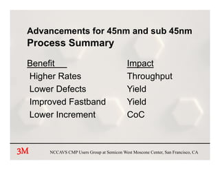
- 20. Advancements for 45nm and sub 45nm Process Summary Benefit Impact Higher Rates Hi h R t Throughput Th h t Lower Defects Yield Improved Fastband Yield Lower Increment CoC 3M NCCAVS CMP Users Group at Semicon West Moscone Center, San Francisco, CA
- 21. Summary and Conclusion • Advances in Chemistry and Abrasive have improved the performance of the FA approach to STI CMP, enabling 45 nm. • A path to achieve key performance needs – lower defects – for sub-45 nm process sub 45 has been identified. 3M NCCAVS CMP Users Group at Semicon West Moscone Center, San Francisco, CA
- 22. Outline Background Timeline of developments leading to Advancements for Sub 45nm p g FA STI CMP Two Step “hybrid” FA Process and Outstanding Planarization Current FA STI CMP Roadmap 65nm, 45nm and Sub 45nm Advancements for 45nm and sub 45nm Chemistry Abrasive CMP Process and performance Summary and C S d Conclusion l i 3 3M NCCAVS CMP Users Group at Semicon West Moscone Center, San Francisco, CA
- 23. Future Venues for 3M CMP Updates • August 2007, Clarkson University CAMP CMP Conference 1. “ADVANCEMENTS IN PAD CONDITIONING FOR TUNGSTEN CHEMICAL MECHANICAL PLANARIZATION” 2. “RECENT ADVANCEMENTS IN FIXED ABRASIVE STI CMP” • September 2007, Semicon Taiwan, Taipei, Taiwan 1. “Mineral, Chemistry and Process Advancements to take Fixed Abrasive STI CMP to sub 45 nm” • October 2007, ICPT Conference, Dresden, Germany 1. “Defectivity Improvement for Fixed Abrasive Based STI CMP in Advanced Logic Technology ” 2. “Laser Scattering Technique for Characterizing Defects and Surface Morphology in the Fixed Abrasive CMP ” 3 3M NCCAVS CMP Users Group at Semicon West Moscone Center, San Francisco, CA
- 24. Advancements For Sub 45nm Fixed Abrasive STI CMP John Gagliardi, Andrey Zagrebelny, Gagliardi Andre Zagrebeln Bill Joseph, Larry Zazzera 3M Company p y 3 3M NCCAVS CMP Users Group at Semicon West Moscone Center, San Francisco, CA