Jk flip flop
- 1. J-K FLIP FLOP & D-FLIP FLOP BY PRIYANK SONI
- 2. WHAT IS FLIP-FLOP? • Flip Flop Circuit can Maintain a binary state indefinitely Until directed by an input signal to switch states. • The Major Differences Among Various types of flip-flops are in the number of inputs .
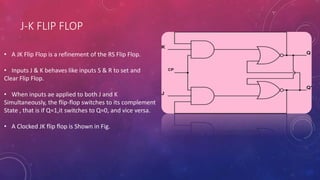
- 3. J-K FLIP FLOP • A JK Flip Flop is a refinement of the RS Flip Flop. • Inputs J & K behaves like inputs S & R to set and Clear Flip Flop. • When inputs ae applied to both J and K Simultaneously, the flip-flop switches to its complement State , that is if Q=1,it switches to Q=0, and vice versa. • A Clocked JK flip flop is Shown in Fig.
- 5. • As Shown in the characteristic table in fig, the J-K Flip Flop behaves like an RS flip flop, expect when both J and K are equal to 1. • When both J and K are 1,the clock pulse is transmitted through one NAND gate Only – the one whose inputs is connected to the flip flop output which is permenetly equal to 1. • If Q=1, the output of the upper AND gate becomes 1 upon application of clock pluse, and the flip flop is cleread. • If Q’=1, the output of lower AND gate becomes a 1 and the flip flop is set . • The output state of the flip flop is complemented.
- 6. D FLIP FLOP: • The D Flip Flop Shown in Fig. is a modification of The clocked RS flip-flop. • The D input goes directly to the S input , and is complement, thorugh gate 5, is applied to The R input. • As long as the clock pulse input is at 0, gates 3 and 4 have a 1 in their outputs. • This Conferms to the requirement that the two inputs of a basic NAND flip flop remain initially at the 1 level.
- 7. • The D input is Sampled during the occurrence of a clock pulse. • If it is 1, the output of Gates 3 goes to 0, switching the flip flop to the set state. • If it is 0,the output of gate 4 goes to 0, switching the flip flop to the clear state. • The D flip flop receives the designation from its ability to transfer “data” into a flip flop. • It is basically an RS flip flop with an inverter in the R inout.
- 9. • This Type of flip flops is sometimes called a gated D-latch. • The clock input is Often given the variable designation G to indicate that this enables the gated latch To make possible the data entry into the flip flop. • The Symbol for a clocked D flip flop is shown in fig. • The Characteristic table is listed in part and the characteristic equation is derived.


