


More Related Content
Similar to Lecture-1.pdf (20)
Recently uploaded (20)


Lecture-1.pdf
- 1. BPHâ106: PHYSICS FOR ENGINEERS Unitâ1 Date: 24.02.2023 Semiconductors Y K Awasthi, PhD Professor-ECE MRIIRS
- 2. Topics to be covered: âĒ Holes and Electrons âĒ Band Theory âĒ Properties of Semiconductors âĒ Types of Semiconductors âĒ Intrinsic Semiconductor âĒ Extrinsic Semiconductor âĒ NâType Semiconductor âĒ PâType Semiconductor âĒ Intrinsic vs Extrinsic âĒ Applications
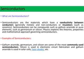
- 3. Semiconductors âĒ What are Semiconductors? âĒ Semiconductors are the materials which have a conductivity between conductors (generally metals) and nonâconductors or insulators (such as ceramics). Semiconductors can be compounds such as gallium arsenide or pure elements, such as germanium or silicon. Physics explains the theories, properties and mathematical approach governing semiconductors. âĒ Examples of Semiconductors: âĒ Gallium arsenide, germanium, and silicon are some of the most commonly used semiconductors. Silicon is used in electronic circuit fabrication and gallium arsenide is used in solar cells, laser diodes, etc.
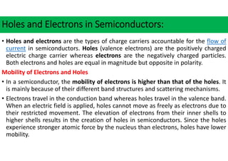
- 4. Holes and Electrons in Semiconductors: âĒ Holes and electrons are the types of charge carriers accountable for the flow of current in semiconductors. Holes (valence electrons) are the positively charged electric charge carrier whereas electrons are the negatively charged particles. Both electrons and holes are equal in magnitude but opposite in polarity. Mobility of Electrons and Holes âĒ In a semiconductor, the mobility of electrons is higher than that of the holes. It is mainly because of their different band structures and scattering mechanisms. âĒ Electrons travel in the conduction band whereas holes travel in the valence band. When an electric field is applied, holes cannot move as freely as electrons due to their restricted movement. The elevation of electrons from their inner shells to higher shells results in the creation of holes in semiconductors. Since the holes experience stronger atomic force by the nucleus than electrons, holes have lower mobility.
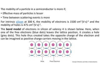
- 5. The mobility of a particle in a semiconductor is more if; âĒ Effective mass of particles is lesser âĒ Time between scattering events is more For intrinsic silicon at 300 K, the mobility of electrons is 1500 cm2 (Vâs)â1 and the mobility of holes is 475 cm2 (Vâs)â1. The bond model of electrons in silicon of valency 4 is shown below. Here, when one of the free electrons (blue dots) leaves the lattice position, it creates a hole (grey dots). This hole thus created takes the opposite charge of the electron and can be imagined as positive charge carriers moving in the lattice.
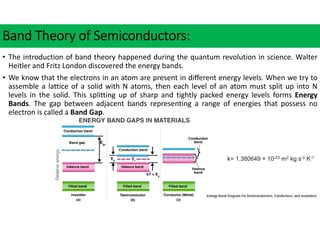
- 6. Band Theory of Semiconductors: âĒ The introduction of band theory happened during the quantum revolution in science. Walter Heitler and Fritz London discovered the energy bands. âĒ We know that the electrons in an atom are present in different energy levels. When we try to assemble a lattice of a solid with N atoms, then each level of an atom must split up into N levels in the solid. This splitting up of sharp and tightly packed energy levels forms Energy Bands. The gap between adjacent bands representing a range of energies that possess no electron is called a Band Gap. k= 1.380649 Ã 10-23 m2 kg s-2 K-1
- 7. Conduction Band and Valence Band in Semiconductors: Valence Band: âĒ The energy band involving the energy levels of valence electrons is known as the valence band. It is the highest occupied energy band. When compared with insulators, the bandgap in semiconductors is smaller. It allows the electrons in the valence band to jump into the conduction band on receiving any external energy. Conduction Band: âĒ It is the lowest unoccupied band that includes the energy levels of positive (holes) or negative (free electrons) charge carriers. It has conducting electrons resulting in the flow of current. The conduction band possess high energy level and are generally empty. The conduction band in semiconductors accepts the electrons from the valence band.
- 8. What is Fermi Level in Semiconductors? âĒ Fermi level (denoted by EF) is present between the valence and conduction bands. It is the highest occupied molecular orbital at absolute zero. The charge carriers in this state have their own quantum states and generally do not interact with each other. When the temperature rises above absolute zero, these charge carriers will begin to occupy states above Fermi level. âĒ In a pâtype semiconductor, there is an increase in the density of unfilled states. Thus, accommodating more electrons at the lower energy levels. However, in an nâtype semiconductor, the density of states increases, therefore, accommodating more electrons at higher energy levels.
- 9. Properties of Semiconductors: âĒ Semiconductors can conduct electricity under preferable conditions or circumstances. This unique property makes it an excellent material to conduct electricity in a controlled manner as required. âĒ Unlike conductors, the charge carriers in semiconductors arise only because of external energy (thermal agitation). It causes a certain number of valence electrons to cross the energy gap and jump into the conduction band, leaving an equal amount of unoccupied energy states, i.e. holes. Conduction due to electrons and holes are equally important. âĒ Resistivity: 10â5 to 106 ÎĐm âĒ Conductivity: 105 to 10â6 mho/m âĒ Temperature coefficient of resistance: Negative âĒ Current Flow: Due to electrons and holes
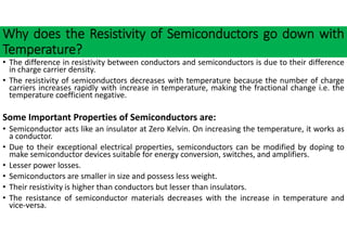
- 10. Why does the Resistivity of Semiconductors go down with Temperature? âĒ The difference in resistivity between conductors and semiconductors is due to their difference in charge carrier density. âĒ The resistivity of semiconductors decreases with temperature because the number of charge carriers increases rapidly with increase in temperature, making the fractional change i.e. the temperature coefficient negative. Some Important Properties of Semiconductors are: âĒ Semiconductor acts like an insulator at Zero Kelvin. On increasing the temperature, it works as a conductor. âĒ Due to their exceptional electrical properties, semiconductors can be modified by doping to make semiconductor devices suitable for energy conversion, switches, and amplifiers. âĒ Lesser power losses. âĒ Semiconductors are smaller in size and possess less weight. âĒ Their resistivity is higher than conductors but lesser than insulators. âĒ The resistance of semiconductor materials decreases with the increase in temperature and viceâversa.
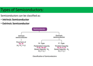
- 11. Types of Semiconductors: Semiconductors can be classified as: âĒ Intrinsic Semiconductor âĒ Extrinsic Semiconductor
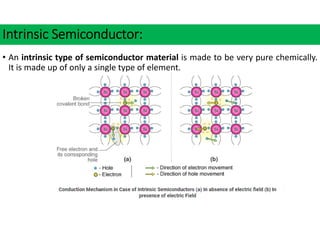
- 12. Intrinsic Semiconductor: âĒ An intrinsic type of semiconductor material is made to be very pure chemically. It is made up of only a single type of element.
- 13. âĒ Germanium (Ge) and Silicon (Si) are the most common type of intrinsic semiconductor elements. They have four valence electrons (tetravalent). They are bound to the atom by covalent bond at absolute zero temperature. âĒ When the temperature rises, due to collisions, few electrons are unbounded and become free to move through the lattice, thus creating an absence in its original position (hole). These free electrons and holes contribute to the conduction of electricity in the semiconductor. The negative and positive charge carriers are equal in number. âĒ The thermal energy is capable of ionizing a few atoms in the lattice, and hence their conductivity is less. The Lattice of Pure Silicon Semiconductor at Different Temperatures: âĒAt absolute zero Kelvin temperature: At this temperature, the covalent bonds are very strong and there are no free electrons and the semiconductor behaves as a perfect insulator. âĒAbove absolute temperature: With the increase in temperature few valence electrons jump into the conduction band and hence it behaves like a poor conductor.
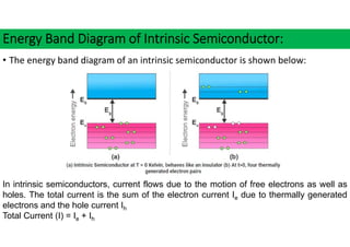
- 14. Energy Band Diagram of Intrinsic Semiconductor: âĒ The energy band diagram of an intrinsic semiconductor is shown below: In intrinsic semiconductors, current flows due to the motion of free electrons as well as holes. The total current is the sum of the electron current Ie due to thermally generated electrons and the hole current Ih Total Current (I) = Ie + Ih
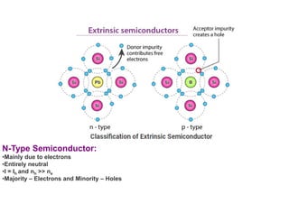
- 15. For an intrinsic semiconductor, at finite temperature, the probability of electrons to exist in conduction band decreases exponentially with increasing bandgap (Eg) n = n0eâEg/2.Kb.T Where, Eg = Energy bandgap Kb = Boltzmannâs constants Extrinsic Semiconductor: The conductivity of semiconductors can be greatly improved by introducing a small number of suitable replacement atoms called IMPURITIES. The process of adding impurity atoms to the pure semiconductor is called DOPING. Usually, only 1 atom in 107 is replaced by a dopant atom in the doped semiconductor. An extrinsic semiconductor can be further classified into: N-type Semiconductor P-type Semiconductor
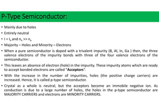
- 16. N-Type Semiconductor: âĒMainly due to electrons âĒEntirely neutral âĒI = Ih and nh >> ne âĒMajority â Electrons and Minority â Holes
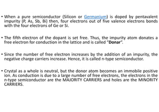
- 17. âĒ When a pure semiconductor (Silicon or Germanium) is doped by pentavalent impurity (P, As, Sb, Bi) then, four electrons out of five valence electrons bonds with the four electrons of Ge or Si. âĒ The fifth electron of the dopant is set free. Thus, the impurity atom donates a free electron for conduction in the lattice and is called âDonarâ. âĒ Since the number of free electron increases by the addition of an impurity, the negative charge carriers increase. Hence, it is called nâtype semiconductor. âĒ Crystal as a whole is neutral, but the donor atom becomes an immobile positive ion. As conduction is due to a large number of free electrons, the electrons in the nâtype semiconductor are the MAJORITY CARRIERS and holes are the MINORITY CARRIERS.
- 18. PâType Semiconductor: âĒ Mainly due to holes âĒ Entirely neutral âĒ I = Ih and nh >> ne âĒ Majority â Holes and Minority â Electrons âĒ When a pure semiconductor is doped with a trivalent impurity (B, Al, In, Ga ) then, the three valence electrons of the impurity bonds with three of the four valence electrons of the semiconductor. âĒ This leaves an absence of electron (hole) in the impurity. These impurity atoms which are ready to accept bonded electrons are called âAcceptorsâ. âĒ With the increase in the number of impurities, holes (the positive charge carriers) are increased. Hence, it is called pâtype semiconductor. âĒ Crystal as a whole is neutral, but the acceptors become an immobile negative ion. As conduction is due to a large number of holes, the holes in the pâtype semiconductor are MAJORITY CARRIERS and electrons are MINORITY CARRIERS.
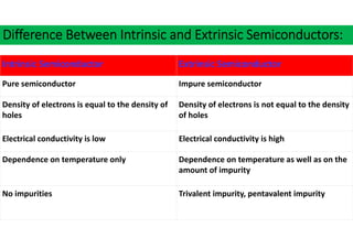
- 19. Difference Between Intrinsic and Extrinsic Semiconductors: Intrinsic Semiconductor Extrinsic Semiconductor Pure semiconductor Impure semiconductor Density of electrons is equal to the density of holes Density of electrons is not equal to the density of holes Electrical conductivity is low Electrical conductivity is high Dependence on temperature only Dependence on temperature as well as on the amount of impurity No impurities Trivalent impurity, pentavalent impurity
- 20. Applications of Semiconductors: âĒ Let us now understand the uses of semiconductors in daily life. Semiconductors are used in almost all electronic devices. Without them, our life would be much different. âĒ Their reliability, compactness, low cost and controlled conduction of electricity make them ideal to be used for various purposes in a wide range of components and devices. transistors, diodes, photosensors, microcontrollers, integrated chips and much more are made up of semiconductors.
- 21. Uses of Semiconductors in Everyday life: âĒ Temperature sensors are made with semiconductor devices. âĒ They are used in 3D printing machines âĒ Used in microchips and selfâdriving cars âĒ Used in calculators, solar plates, computers and other electronic devices. âĒ Transistor and MOSFET used as a switch in Electrical Circuits are manufactured using the semiconductors.
- 22. Industrial Uses of Semiconductors: âĒ The physical and chemical properties of semiconductors make them capable of designing technological wonders like microchips, transistors, LEDs, solar cells, etc. âĒ The microprocessor used for controlling the operation of space vehicles, trains, robots, etc is made up of transistors and other controlling devices which are manufactured by semiconductor materials. Importance of Semiconductors: âĒ Here we have discussed some advantages of semiconductors which makes them highly useful everywhere. âĒ They are highly portable due to the smaller size âĒ They require less input power âĒ Semiconductor devices are shockproof âĒ They have a longer lifespan âĒ They are noiseâfree while operating