Lecture3 IC fabrication process
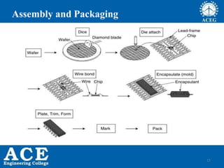
- 2. IC Fabrication Process Sequence âąSilicon Wafer manufacturing âąWafer processing âąOxidation âąPhoto Lithography âąEtching âąDiffusion & Ion implantation âąMetallization âąTesting âąAssembly and packaging
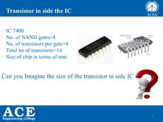
- 3. 3 Transistor in side the IC IC 7400 No. of NAND gates=4 No. of transistors per gate=4 Total no of transistors=16 Size of chip in terms of mm Can you Imagine the size of the transistor in side IC
- 4. IC Fabrication Process- Video from Intel âFrom sand to siliconâ in youtube
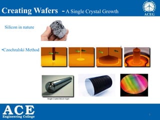
- 5. 5 Creating Wafers -A Single Crystal Growth âąCzochralski Method Silicon in nature
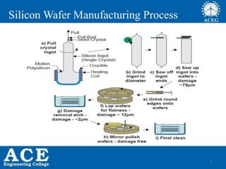
- 6. 6 Silicon Wafer Manufacturing Process
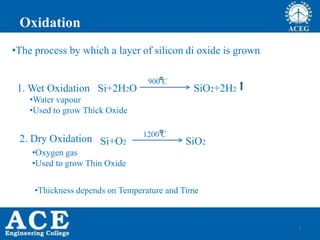
- 7. 7 Oxidation Si+O2 SiO2 1200 C 1. Wet Oxidation âąWater vapour âąUsed to grow Thick Oxide âąOxygen gas âąUsed to grow Thin Oxide 2. Dry Oxidation Si+2H2O SiO2+2H2 900 C âąThickness depends on Temperature and Time âąThe process by which a layer of silicon di oxide is grown
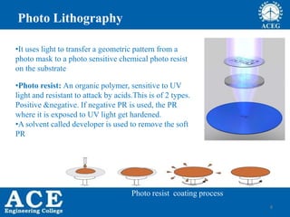
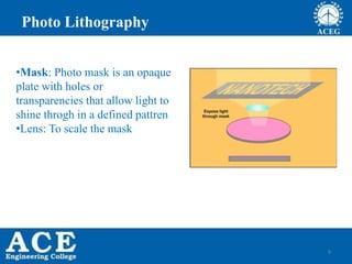
- 8. 8 Photo Lithography âąIt uses light to transfer a geometric pattern from a photo mask to a photo sensitive chemical photo resist on the substrate âąPhoto resist: An organic polymer, sensitive to UV light and resistant to attack by acids.This is of 2 types. Positive &negative. If negative PR is used, the PR where it is exposed to UV light get hardened. âąA solvent called developer is used to remove the soft PR Photo resist coating process
- 9. 9 âąMask: Photo mask is an opaque plate with holes or transparencies that allow light to shine throgh in a defined pattren âąLens: To scale the mask Photo Lithography
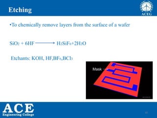
- 10. 10 Etching Etchants: KOH, HF,BF6,BCl3 SiO2 + 6HF H2SiF6+2H2O âąTo chemically remove layers from the surface of a wafer
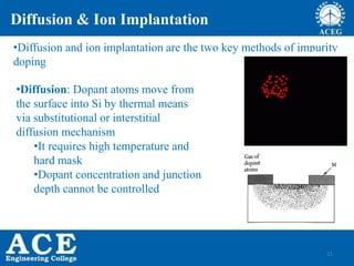
- 11. 11 Diffusion & Ion Implantation âąDiffusion and ion implantation are the two key methods of impurity doping âąDiffusion: Dopant atoms move from the surface into Si by thermal means via substitutional or interstitial diffusion mechanism âąIt requires high temperature and hard mask âąDopant concentration and junction depth cannot be controlled
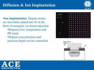
- 12. 12 âąIon implantation: Dopant atoms are forcefully added into Si in the form of energetic ion beam injection âąRequires low temperature and PR mask âąDopant concentration and junction depth can be controlled Diffusion & Ion Implantation
- 13. 13 Metallization âąProvides contacts and interconnections âąMost commonly used material- Aluminium âąRequirements âąLow resistance Ohmic contacts âąLow sheet resistance âąReliable interconnections
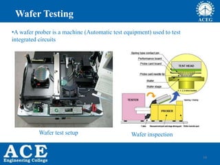
- 14. 14 Wafer Testing âąA wafer prober is a machine (Automatic test equipment) used to test integrated circuits Wafer test setup Wafer inspection
