M O C V Dmaterialgrowth
- 1. MOCVD technology and material growth Introduction The MOVD technique and growth system Metalorganic compound Gas phase and surface reaction Materials Characterization MOCVD growth of GaN
- 2. 1.Introduction Most of the advances in semiconductor processing have centered on the ability to decrease the physical dimensions of the electronic device structure. Â Lateral dimension: Photolithographic, Deposition Etching techniquesâĶ Vertical dimension: Epitaxial deposition
- 3. Compare of epitaxial methods Some of the sources like AsH 3 are very toxic. Use metalorganic compounds as the sources 1968 MOCVD (Metal-Organic Chemical Vapor Deposition) Hard to grow materials with high vapor pressure Deposit epilayer at ultrahigh vacuum 1958 1967 MBE (Molecular Beam Epitaxy) No Al contained compound, thick layer Use metal halide as transport agents to grow 1958 VPE (Vapor phase epitaxy Limited substrate areas and poor control over the growth of very thin layers Growth form supersaturated solution onto substrate 1963 LPE (Liquid phase epitaxy) limit features time Growth method
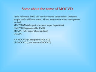
- 4. Some about the name of MOCVD In the reference, MOCVD also have some other names. Different people prefer different name. All the names refer to the same growth method. MOCVD (Metalorganic chemical vapor deposition) OMCVD(Organometallic CVD) MOVPE (MO vapor phase epitaxy) OMVPE AP-MOCVD (Atmosphere MOCVD) LP-MOCVD (Low pressure MOCVD)
- 5. 2. The MOVD growth system
- 6. MOCVD Growth System Vacuum and Exhaust system Gas handle system Computer Control Reactor
- 7. Gas handling system The function of gas handling system is mixing and metering of the gas that will enter the reactor. Timing and composition of the gas entering the reactor will determine the epilayer structure.  Leak-tight of the gas panel is essential, because the oxygen contamination will degrade the growing filmsâ properties. Fast switch of valve system is very important for thin film and abrupt interface structure growth,  Accurate control of flow rate, pressure and temperature can ensure the stable and repeat.
- 8. Reactor-1
- 9. Reactor-2
- 11. Exhaust system Pump and pressure controller For low pressure growth, we use mechanic pump and pressure controller to control the growth pressure. The pump should be designed to handle large gas load. waste gas treatment system The treatment of exhaust gas is a matter of safety concern. The MOCVD system for GaAs and InP use toxic materials like AsH 3 and PH 3 . The exhaust gases still contain some not reacted AsH 3 and PH 3 , Normally, the toxic gas need to be removed by using chemical scrubber. For GaN system, it is not a problem.
- 12. 3. Metalorganic compound The vapor pressure of the MO source is an important consideration in MOCVD, since it determines the concentration of source material in the reactor and the deposition rate. Too low a vapor pressure makes it difficult to transport the source into the deposition zone and to achieve reasonable growth rates. Too high a vapor pressure may raise safety concerns if the compound is toxic. Further more, it is easier to control the delivery from a liquid than from a solid. Vapor pressures of Metalorganic compounds are calculated in terms of the expression  Log[p(torr)]=B-A/T
- 13. Vapor pressure of most common MO compounds Log[p(torr)]=B-A/T Cp2Mg DEZn TEIn TMIn TEGa TMGa TEAl TMAl 175 10.56 3556 0.05 Mg(C 5 H 5 ) 2 -28 8.28 2190 8.53 Zn(C 2 H 5 ) 2 -32 8.94 2815 0.31 In(C 2 H 5 ) 3 88 9.74 2830 1.75 In(CH3) 3 -82.5 9.19 2530 4.79 Ga(C 2 H 5 ) 3 -15.8 8.50 1825 238 Ga(CH 3 ) 3 -52.5 10.78 3625 0.041 Al(C 2 H 5 ) 3 15 10.48 2780 14.2 (Al(CH 3 ) 3 ) 2 Melt point ( o C) B A P at 298 K (torr) Compound
- 14. Calculate the mole flow rate of MO sources When we read some reference, we often see people use mol/min to indicate the flow rate. Normally, we use the formula to calculate it. Â F (mol/min)=p MO /p Bubbler *[flow rate (ml/min)]/22400 (mol/ml) Â We need to calculate the mole flow rate before we determine the growth condition. If we want to grow alloys, we can use the mole flow rate to estimate the alloysâ composition. For example, if we grow AlGaN, we can estimate the Al concentration use the following formula if we assume the efficiency of Al and Ga sources is the same. x Al =F Al /(F Al + F Ga )
- 15. 4. Gas phase and surface reaction The basic reaction describe GaN growth can simply write as Ga(CH 3 ) 3 +NH 3 ï GaN+3CH 4 The growth procedure as follows: MO sources and hydrides inject to the reactor. The sources are mixed inside the reactor and transfer to the deposition area At the deposition area, high temperature result in the decomposition of sources and other gas-phase reaction, forming the film precursors which are useful for film growth and by-products. The film precursors transport to the growth surface The film precursors absorb on the growth surface The film precursors diffuse to the growth site At the surface, film atoms incorporate into the growing film through surface reaction The by-products of the surface reactions absorb from surface The by-products transport to the main gas flow region away from the deposition area towards the reactor exit
- 16. reaction
- 17. 5. Materials Characterization Physical characterization X-ray diffraction (XDS) Transmission electron microscopy (TEM) Optical microscopy Scanning electron microscopy (SEM) Atom force microscopy (AFM) Secondary ion mass spectroscopy (SIMS) Electrical Measurements Van der Pauw Hall Capacitance-voltage (C-V) Optical measurements Photoluminescence (PL)
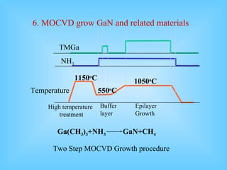
- 18. 6. MOCVD grow GaN and related materials Two Step MOCVD Growth procedure Ga(CH 3 ) 3 +NH 3 GaN+CH 4 High temperature treatment Buffer layer Epilayer Growth TMGa NH 3 Temperature 1150 o C 550 o C 1050 o C
- 19. Some basic problem related to GaN growth MOCVD and other epitaxial techniques have developed more than 30 years, but high quality GaN and related compound only available in recent years. There are some special problems for GaN and related materials. No suitable substrate Difficult to obtain p-type epilayer


![3. Metalorganic compound The vapor pressure of the MO source is an important consideration in MOCVD, since it determines the concentration of source material in the reactor and the deposition rate. Too low a vapor pressure makes it difficult to transport the source into the deposition zone and to achieve reasonable growth rates. Too high a vapor pressure may raise safety concerns if the compound is toxic. Further more, it is easier to control the delivery from a liquid than from a solid. Vapor pressures of Metalorganic compounds are calculated in terms of the expression  Log[p(torr)]=B-A/T](https://image.slidesharecdn.com/mocvdmaterialgrowth-1299860544-phpapp01/85/M-O-C-V-Dmaterialgrowth-12-320.jpg)
![Vapor pressure of most common MO compounds Log[p(torr)]=B-A/T Cp2Mg DEZn TEIn TMIn TEGa TMGa TEAl TMAl 175 10.56 3556 0.05 Mg(C 5 H 5 ) 2 -28 8.28 2190 8.53 Zn(C 2 H 5 ) 2 -32 8.94 2815 0.31 In(C 2 H 5 ) 3 88 9.74 2830 1.75 In(CH3) 3 -82.5 9.19 2530 4.79 Ga(C 2 H 5 ) 3 -15.8 8.50 1825 238 Ga(CH 3 ) 3 -52.5 10.78 3625 0.041 Al(C 2 H 5 ) 3 15 10.48 2780 14.2 (Al(CH 3 ) 3 ) 2 Melt point ( o C) B A P at 298 K (torr) Compound](https://image.slidesharecdn.com/mocvdmaterialgrowth-1299860544-phpapp01/85/M-O-C-V-Dmaterialgrowth-13-320.jpg)
![Calculate the mole flow rate of MO sources When we read some reference, we often see people use mol/min to indicate the flow rate. Normally, we use the formula to calculate it. Â F (mol/min)=p MO /p Bubbler *[flow rate (ml/min)]/22400 (mol/ml) Â We need to calculate the mole flow rate before we determine the growth condition. If we want to grow alloys, we can use the mole flow rate to estimate the alloysâ composition. For example, if we grow AlGaN, we can estimate the Al concentration use the following formula if we assume the efficiency of Al and Ga sources is the same. x Al =F Al /(F Al + F Ga )](https://image.slidesharecdn.com/mocvdmaterialgrowth-1299860544-phpapp01/85/M-O-C-V-Dmaterialgrowth-14-320.jpg)


