ME LAB1.docx
Download as docx, pdf0 likes11 views

This document describes modeling sequential digital systems using Verilog and provides examples of modeling various sequential logic circuits including D flip-flops, T flip-flops, JK flip-flops, and mod-7 counters. It outlines the steps to create a project in Xilinx ISE, write the Verilog code, and simulate the models. Code examples are provided for a D flip-flop, T flip-flop, JK flip-flop, mod-7 down counter, and mod-7 up counter. The document also discusses shift register operation and provides two examples of VHDL code to create an 8-bit shift register.
![4.MOD-7 DOWN COUNTER:
BLOCK DIAGRAM: TRUTH TABLE:
Clk rst [2:0]q
1 1 1 1 1
1 0 1 1 0
1 0 1 0 1
1 0 1 0 0
1 0 0 1 1
1 0 0 1 0
1 0 0 0 1
1 0 0 0 0](https://image.slidesharecdn.com/melab1-220913164952-cb78ae69/85/ME-LAB1-docx-2-320.jpg)

![PROGRAM:
module count(clk, rst, count);
input clk;
input rst;
output [3:0] count;
reg [3:0] count;
always @ (posedge clk)
begin
if (rst)
count <= "1111";](https://image.slidesharecdn.com/melab1-220913164952-cb78ae69/85/ME-LAB1-docx-4-320.jpg)

![5.MOD-7 UP COUNTER:
BLOCK DIAGRAM: TRUTH TABLE:
SIMULATED OUTPUT:
PROGRAM:
module vp1(clk, rst, a);
input clk;
input rst;
output [2:0] a;
reg[2:0] a;
always@(posedge clk)
begin
if(rst)
a="000";
else
a=a+1;
end
endmodule
Clk rst [2:0]q
1 1 0 0 0
1 0 0 0 1
1 0 0 1 0
1 0 0 1 1
1 0 1 0 0
1 0 1 0 1
1 0 1 1 0
1 0 1 1 1](https://image.slidesharecdn.com/melab1-220913164952-cb78ae69/85/ME-LAB1-docx-6-320.jpg)

ME LAB1.docx
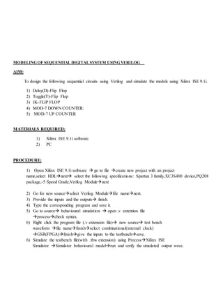
- 1. MODELING OF SEQUENTIAL DIGITALSYSTEM USING VERILOG AIM: To design the following sequential circuits using Verilog and simulate the models using Xilinx ISE 9.1i. 1) Delay(D)-Flip Flop 2) Toggle(T)-Flip Flop 3) JK-FLIP FLOP 4) MOD-7 DOWN COUNTER: 5) MOD-7 UP COUNTER MATERIALS REQUIRED: 1) Xilinx ISE 9.1i software. 2) PC PROCEDURE: 1) Open Xilinx ISE 9.1i software ï go to file ï create new project with an project name,select HDLï nextï select the following specifications: Spartan 3 family,XC3S400 device,PQ208 package,-5 Speed Grade,Verilog Moduleï next 2) Go for new sourceï select Verilog Moduleï file nameï next. 3) Provide the inputs and the outputsï finish. 4) Type the corresponding program and save it. 5) Go to sourceï behavioural simulation ï open .v extention file ï processï check syntax. 6) Right click the program file (.v extension file)ï new sourceï test bench waveform ï file nameï finishï select combinational(internal clock) ï GSR(FPGA)ï finishï give the inputs to the testbenchï save. 6) Simulate the testbench file(with .tbw extension) using Processï Xilinx ISE Simulator ï Simulator behavioural modelï run and verify the simulated output wave.
- 2. 4.MOD-7 DOWN COUNTER: BLOCK DIAGRAM: TRUTH TABLE: Clk rst [2:0]q 1 1 1 1 1 1 0 1 1 0 1 0 1 0 1 1 0 1 0 0 1 0 0 1 1 1 0 0 1 0 1 0 0 0 1 1 0 0 0 0
- 4. PROGRAM: module count(clk, rst, count); input clk; input rst; output [3:0] count; reg [3:0] count; always @ (posedge clk) begin if (rst) count <= "1111";
- 6. 5.MOD-7 UP COUNTER: BLOCK DIAGRAM: TRUTH TABLE: SIMULATED OUTPUT: PROGRAM: module vp1(clk, rst, a); input clk; input rst; output [2:0] a; reg[2:0] a; always@(posedge clk) begin if(rst) a="000"; else a=a+1; end endmodule Clk rst [2:0]q 1 1 0 0 0 1 0 0 0 1 1 0 0 1 0 1 0 0 1 1 1 0 1 0 0 1 0 1 0 1 1 0 1 1 0 1 0 1 1 1
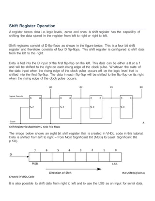
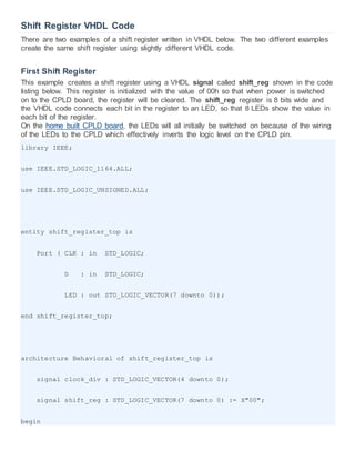
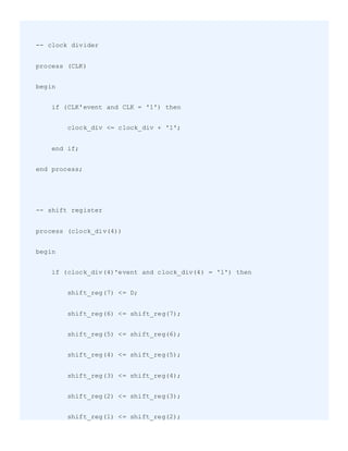
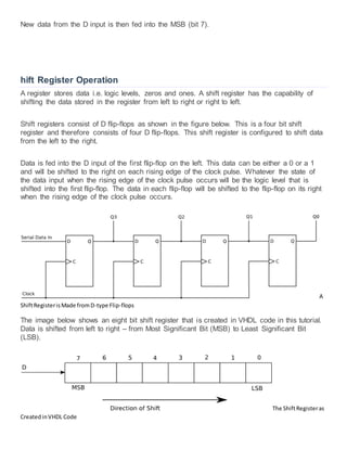
- 8. Shift Register Operation A register stores data i.e. logic levels, zeros and ones. A shift register has the capability of shifting the data stored in the register from left to right or right to left. Shift registers consist of D flip-flops as shown in the figure below. This is a four bit shift register and therefore consists of four D flip-flops. This shift register is configured to shift data from the left to the right. Data is fed into the D input of the first flip-flop on the left. This data can be either a 0 or a 1 and will be shifted to the right on each rising edge of the clock pulse. Whatever the state of the data input when the rising edge of the clock pulse occurs will be the logic level that is shifted into the first flip-flop. The data in each flip-flop will be shifted to the flip-flop on its right when the rising edge of the clock pulse occurs. A ShiftRegisterisMade fromD-type Flip-flops The image below shows an eight bit shift register that is created in VHDL code in this tutorial. Data is shifted from left to right â from Most Significant Bit (MSB) to Least Significant Bit (LSB). The ShiftRegisteras CreatedinVHDL Code It is also possible to shift data from right to left and to use the LSB as an input for serial data.
- 9. Shift Register VHDL Code There are two examples of a shift register written in VHDL below. The two different examples create the same shift register using slightly different VHDL code. First Shift Register This example creates a shift register using a VHDL signal called shift_reg shown in the code listing below. This register is initialized with the value of 00h so that when power is switched on to the CPLD board, the register will be cleared. The shift_reg register is 8 bits wide and the VHDL code connects each bit in the register to an LED, so that 8 LEDs show the value in each bit of the register. On the home built CPLD board, the LEDs will all initially be switched on because of the wiring of the LEDs to the CPLD which effectively inverts the logic level on the CPLD pin. library IEEE; use IEEE.STD_LOGIC_1164.ALL; use IEEE.STD_LOGIC_UNSIGNED.ALL; entity shift_register_top is Port ( CLK : in STD_LOGIC; D : in STD_LOGIC; LED : out STD_LOGIC_VECTOR(7 downto 0)); end shift_register_top; architecture Behavioral of shift_register_top is signal clock_div : STD_LOGIC_VECTOR(4 downto 0); signal shift_reg : STD_LOGIC_VECTOR(7 downto 0) := X"00"; begin
- 10. -- clock divider process (CLK) begin if (CLK'event and CLK = '1') then clock_div <= clock_div + '1'; end if; end process; -- shift register process (clock_div(4)) begin if (clock_div(4)'event and clock_div(4) = '1') then shift_reg(7) <= D; shift_reg(6) <= shift_reg(7); shift_reg(5) <= shift_reg(6); shift_reg(4) <= shift_reg(5); shift_reg(3) <= shift_reg(4); shift_reg(2) <= shift_reg(3); shift_reg(1) <= shift_reg(2);
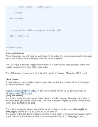
- 11. shift_reg(0) <= shift_reg(1); end if; end process; -- hook up the shift register bits to the LEDs LED <= shift_reg; end Behavioral; Inputs and Outputs The shift register has a D input for serial data. In the video, this input is connected to the right switch of the switch bank and feeds data into the shift register. The CLK input of the shift register is connected to a clock source. Data is shifted in the shift register on each rising edge of the clock pulse. The LED outputs connect each bit in the shift register to its own LED on the CPLD board. Clock Divider A clock divider is used to slow down the input clock so that the contents of the shift register will be visible on the LEDs. Tutorial 6 (Clock Divider in VHDL) in this course shows how to set up the input clock for the home made CPLD board. Doing the Shifting The shifting inside the shift register takes place in a VHDL process. On every rising edge of the clock pulse (the divided clock pulse), the data in the shift register is shifted one bit to the right â from the MSB to the LSB. The shifting is done by moving each bit to the bit position to its right, e.g. shift_reg(6) <= shift_reg(7); moves bit 7 to bit 6, and so on for each bit. The source of the data being shifted is from the D input which is connected to a switch on the board. The D input is fed to the MSB of the shift register (i.e. bit 7): shift_reg(7) <= D;
- 12. Second Shift Register The second VHDL shift register, shown below, works in exactly the same way as the first shift register except that the shifting process is simplified. library IEEE; use IEEE.STD_LOGIC_1164.ALL; use IEEE.STD_LOGIC_UNSIGNED.ALL; entity shift_register2 is Port ( D : in STD_LOGIC; CLK : in STD_LOGIC; LED : out STD_LOGIC_VECTOR (7 downto 0)); end shift_register2; architecture Behavioral of shift_register2 is signal clock_div : STD_LOGIC_VECTOR(4 downto 0); signal shift_reg : STD_LOGIC_VECTOR(7 downto 0) := X"00"; begin -- clock divider process (CLK) begin
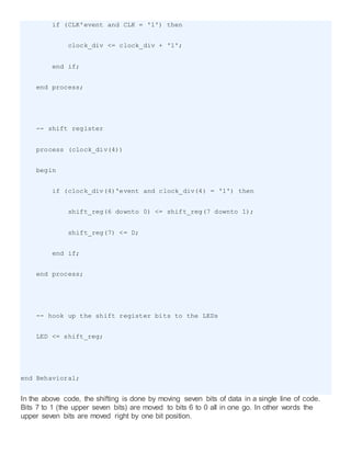
- 13. if (CLK'event and CLK = '1') then clock_div <= clock_div + '1'; end if; end process; -- shift register process (clock_div(4)) begin if (clock_div(4)'event and clock_div(4) = '1') then shift_reg(6 downto 0) <= shift_reg(7 downto 1); shift_reg(7) <= D; end if; end process; -- hook up the shift register bits to the LEDs LED <= shift_reg; end Behavioral; In the above code, the shifting is done by moving seven bits of data in a single line of code. Bits 7 to 1 (the upper seven bits) are moved to bits 6 to 0 all in one go. In other words the upper seven bits are moved right by one bit position.
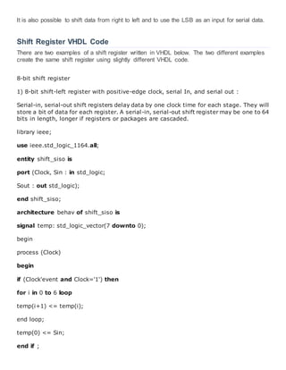
- 14. New data from the D input is then fed into the MSB (bit 7). hift Register Operation A register stores data i.e. logic levels, zeros and ones. A shift register has the capability of shifting the data stored in the register from left to right or right to left. Shift registers consist of D flip-flops as shown in the figure below. This is a four bit shift register and therefore consists of four D flip-flops. This shift register is configured to shift data from the left to the right. Data is fed into the D input of the first flip-flop on the left. This data can be either a 0 or a 1 and will be shifted to the right on each rising edge of the clock pulse. Whatever the state of the data input when the rising edge of the clock pulse occurs will be the logic level that is shifted into the first flip-flop. The data in each flip-flop will be shifted to the flip-flop on its right when the rising edge of the clock pulse occurs. A ShiftRegisterisMade fromD-type Flip-flops The image below shows an eight bit shift register that is created in VHDL code in this tutorial. Data is shifted from left to right â from Most Significant Bit (MSB) to Least Significant Bit (LSB). The ShiftRegisteras CreatedinVHDL Code
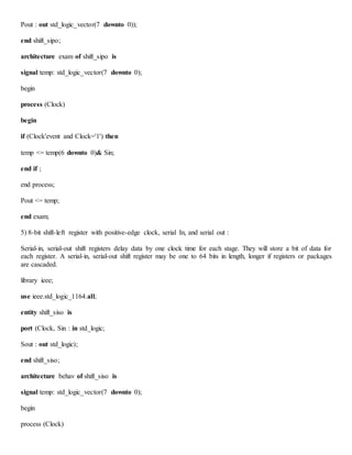
- 15. It is also possible to shift data from right to left and to use the LSB as an input for serial data. Shift Register VHDL Code There are two examples of a shift register written in VHDL below. The two different examples create the same shift register using slightly different VHDL code. 8-bit shift register 1) 8-bit shift-left register with positive-edge clock, serial In, and serial out : Serial-in, serial-out shift registers delay data by one clock time for each stage. They will store a bit of data for each register. A serial-in, serial-out shift register may be one to 64 bits in length, longer if registers or packages are cascaded. library ieee; use ieee.std_logic_1164.all; entity shift_siso is port (Clock, Sin : in std_logic; Sout : out std_logic); end shift_siso; architecture behav of shift_siso is signal temp: std_logic_vector(7 downto 0); begin process (Clock) begin if (Clock'event and Clock='1') then for i in 0 to 6 loop temp(i+1) <= temp(i); end loop; temp(0) <= Sin; end if ;
- 16. end process; Sout <= temp(7); end behav; 2) 8-bit shift-left register with positive-edge clock, asynchronous clear, serial in, and serial out : library ieee; use ieee.std_logic_1164.all; entity shift_siso is port (Clock, Sin, Clear : in std_logic; Sout : out std_logic); end shift_siso; architecture behav of shift_siso is signal temp: std_logic_vector(7 downto 0); begin process (Clock, Clear) begin if (Clear='1') then temp <= (others => '0'); elsif (Clock'event and Clock='1') then temp <= temp(6 downto 0) & Sin; end if ; end process; Sout <= temp(7); end behav; 3) 8-bit shift-left register with positive-edge clock, synchronous set, serial In, and serial out :
- 17. library ieee; use ieee.std_logic_1164.all; entity shift_SS is port (Clock, Sin, Set : in std_logic; Sout : out std_logic); end shift_SS; architecture behav of shift_SS is signal temp: std_logic_vector(7 downto 0); begin process (Clock, Set) begin if (Clock'event and Clock='1') then if (Set='1') then temp <= (others => '1'); else temp <= temp(6 downto 0) & Sin; end if ; end if ; end process; Sout <= temp(7); end behav; 4) 8-bit shift-left register with positive-edge clock, serial in, and parallel out : library ieee; use ieee.std_logic_1164.all; entity shift_sipo is port (Clock, Sin : in std_logic;
- 18. Pout : out std_logic_vector(7 downto 0)); end shift_sipo; architecture exam of shift_sipo is signal temp: std_logic_vector(7 downto 0); begin process (Clock) begin if (Clock'event and Clock='1') then temp <= temp(6 downto 0)& Sin; end if ; end process; Pout <= temp; end exam; 5) 8-bit shift-left register with positive-edge clock, serial In, and serial out : Serial-in, serial-out shift registers delay data by one clock time for each stage. They will store a bit of data for each register. A serial-in, serial-out shift register may be one to 64 bits in length, longer if registers or packages are cascaded. library ieee; use ieee.std_logic_1164.all; entity shift_siso is port (Clock, Sin : in std_logic; Sout : out std_logic); end shift_siso; architecture behav of shift_siso is signal temp: std_logic_vector(7 downto 0); begin process (Clock)
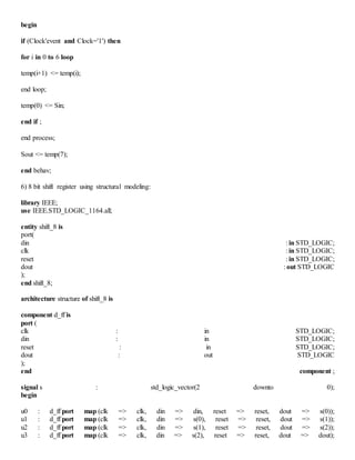
- 19. begin if (Clock'event and Clock='1') then for i in 0 to 6 loop temp(i+1) <= temp(i); end loop; temp(0) <= Sin; end if ; end process; Sout <= temp(7); end behav; 6) 8 bit shift register using structural modeling: library IEEE; use IEEE.STD_LOGIC_1164.all; entity shift_8 is port( din : in STD_LOGIC; clk : in STD_LOGIC; reset : in STD_LOGIC; dout : out STD_LOGIC ); end shift_8; architecture structure of shift_8 is component d_ff is port ( clk : in STD_LOGIC; din : in STD_LOGIC; reset : in STD_LOGIC; dout : out STD_LOGIC ); end component ; signal s : std_logic_vector(2 downto 0); begin u0 : d_ff port map (clk => clk, din => din, reset => reset, dout => s(0)); u1 : d_ff port map (clk => clk, din => s(0), reset => reset, dout => s(1)); u2 : d_ff port map (clk => clk, din => s(1), reset => reset, dout => s(2)); u3 : d_ff port map (clk => clk, din => s(2), reset => reset, dout => dout);
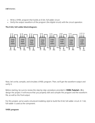
- 20. end structure; ï· Write a VHDL program that builds an 8-bit, full-adder circuit ï· Verify the output waveform of the program (the digital circuit) with the circuit operation The 8-bit, full-adder block diagram: Now, letâs write, compile, and simulate a VHDL program. Then, weâll get the waveform output and verify it. Before starting, be sure to review the step-by-step procedure provided in VHDL Tutorial â 3 to design the project. It will ensure that you properly edit and compile the program and the waveform file, as well as the final output. For this project, weâve used a structural modeling style to build the 8-bit, full-adder circuit. A 1-bit, full-adder is used as the component. VHDL program
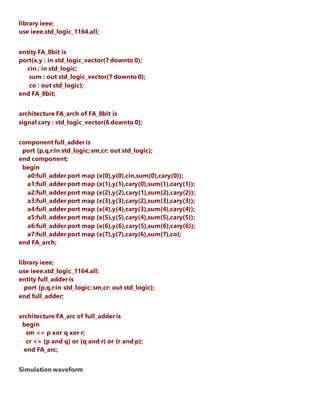
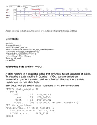
- 21. library ieee; use ieee.std_logic_1164.all; entity FA_8bit is port(x,y : in std_logic_vector(7 downto 0); cin : in std_logic; sum : out std_logic_vector(7 downto 0); co : out std_logic); end FA_8bit; architecture FA_arch of FA_8bit is signal cary : std_logic_vector(6 downto 0); component full_adder is port (p,q,r:in std_logic; sm,cr: out std_logic); end component; begin a0:full_adder port map (x(0),y(0),cin,sum(0),cary(0)); a1:full_adder port map (x(1),y(1),cary(0),sum(1),cary(1)); a2:full_adder port map (x(2),y(2),cary(1),sum(2),cary(2)); a3:full_adder port map (x(3),y(3),cary(2),sum(3),cary(3)); a4:full_adder port map (x(4),y(4),cary(3),sum(4),cary(4)); a5:full_adder port map (x(5),y(5),cary(4),sum(5),cary(5)); a6:full_adder port map (x(6),y(6),cary(5),sum(6),cary(6)); a7:full_adder port map (x(7),y(7),cary(6),sum(7),co); end FA_arch; library ieee; use ieee.std_logic_1164.all; entity full_adder is port (p,q,r:in std_logic; sm,cr: out std_logic); end full_adder; architecture FA_arc of full_adder is begin sm <= p xor q xor r; cr <= (p and q) or (q and r) or (r and p); end FA_arc; Simulation waveform
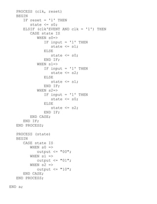
- 22. As can be noted in this figure, the sum of x, y, and cin are highlighted in red and blue. MULTIPLIERS Multiplierâ Top Level libraryIEEE; use IEEE.STD_LOGIC_1164.ALL; entityMultTopisport ( Multiplier:instd_logic_vector(3downto0); Multiplicand:instd_logic_vector(3downto0); Product:out std_logic_vector(7downto0); Start: instd_logic;Clk:instd_logic; Done:out std_logic); endMultTop; mplementing State Machines (VHDL) A state machine is a sequential circuit that advances through a number of states. To describe a state machine in Quartus II VHDL, you can declare an enumeration type for the states, and use a Process Statement for the state register and the next-state logic. The VHDL example shown below implements a 3-state state machine. ENTITY state_machine IS PORT( clk : IN STD_LOGIC; input : IN STD_LOGIC; reset : IN STD_LOGIC; output : OUT STD_LOGIC_VECTOR(1 downto 0)); END state_machine; ARCHITECTURE a OF state_machine IS TYPE STATE_TYPE IS (s0, s1, s2); SIGNAL state : STATE_TYPE; BEGIN
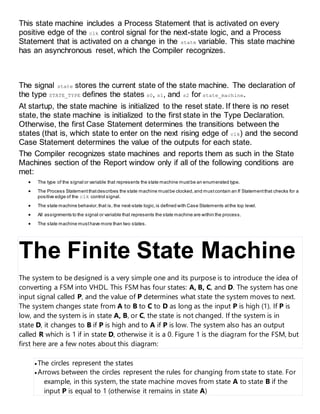
- 23. PROCESS (clk, reset) BEGIN IF reset = '1' THEN state <= s0; ELSIF (clk'EVENT AND clk = '1') THEN CASE state IS WHEN s0=> IF input = '1' THEN state <= s1; ELSE state <= s0; END IF; WHEN s1=> IF input = '1' THEN state <= s2; ELSE state <= s1; END IF; WHEN s2=> IF input = '1' THEN state <= s0; ELSE state <= s2; END IF; END CASE; END IF; END PROCESS; PROCESS (state) BEGIN CASE state IS WHEN s0 => output <= "00"; WHEN s1 => output <= "01"; WHEN s2 => output <= "10"; END CASE; END PROCESS; END a;
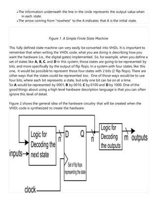
- 24. This state machine includes a Process Statement that is activated on every positive edge of the clk control signal for the next-state logic, and a Process Statement that is activated on a change in the state variable. This state machine has an asynchronous reset, which the Compiler recognizes. The signal state stores the current state of the state machine. The declaration of the type STATE_TYPE defines the states s0, s1, and s2 for state_machine. At startup, the state machine is initialized to the reset state. If there is no reset state, the state machine is initialized to the first state in the Type Declaration. Otherwise, the first Case Statement determines the transitions between the states (that is, which state to enter on the next rising edge of clk) and the second Case Statement determines the value of the outputs for each state. The Compiler recognizes state machines and reports them as such in the State Machines section of the Report window only if all of the following conditions are met: ï· The type of the signal or variable that represents the state machine mustbe an enumerated type. ï· The Process Statementthatdescribes the state machine mustbe clocked,and mustcontain an If Statementthat checks for a positive edge of the clk control signal. ï· The state machine behavior,that is, the next-state logic,is defined with Case Statements atthe top level. ï· All assignments to the signal or variable that represents the state machine are within the process. ï· The state machine musthave more than two states. The Finite State Machine The system to be designed is a very simple one and its purpose is to introduce the idea of converting a FSM into VHDL. This FSM has four states: A, B, C, and D. The system has one input signal called P, and the value of P determines what state the system moves to next. The system changes state from A to B to C to D as long as the input P is high (1). If P is low, and the system is in state A, B, or C, the state is not changed. If the system is in state D, it changes to B if P is high and to A if P is low. The system also has an output called R which is 1 if in state D, otherwise it is a 0. Figure 1 is the diagram for the FSM, but first here are a few notes about this diagram: ï· The circles represent the states ï· Arrows between the circles represent the rules for changing from state to state. For example, in this system, the state machine moves from state A to state B if the input P is equal to 1 (otherwise it remains in state A)
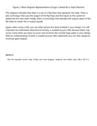
- 25. ï· The information underneath the line in the circle represents the output value when in each state. ï· The arrow coming from "nowhere" to the A indicates that A is the initial state. Figure 1. A Simple Finite State Machine This fully defined state machine can very easily be converted into VHDL. It is important to remember that when writing the VHDL code, what you are doing is describing how you want the hardware (i.e., the digital gates) implemented. So, for example, when you define a set of states like A, B, C, and D in this system, those states are going to be represented by bits, and more specifically by the output of flip flops. In a system with four states, like this one, it would be possible to represent those four states with 2 bits (2 flip flops). There are other ways that the states could be represented too. One of those ways would be to use four bits, where each bit represents a state, but only one bit can be on at a time. So A would be represented by 0001, B by 0010, C by 0100 and D by 1000. One of the good things about using a high level hardware description language is that you can often ignore this level of detail. Figure 2 shows the general idea of the hardware circuitry that will be created when the VHDL code is synthesized to create the hardware.
- 26. Figure 2. Block Diagram Representation of Logic Created for a State Machine This diagram indicates that there is a set of n flip flops that represent the state. There is also some logic that uses the output of the flip flops and the inputs to the system to determine the next state. Finally, there is some logic that decodes the output values of the flip flops to create the m output signals. Again, when using a HDL, you can often ignore this level of detail in your design. It is still important to understand what kind of circuitry is created by your HDL because there may come a time when you have to count and minimize the number logic gates in your design. With an understanding of what is created by your HDL statements you can then design to minimize gate creation. RESULT: Thus the sequential circuits using Verilog have been designed, simulated and verified using Xilinx ISE 9.1i.