The document describes examples of cache coherence protocols including MSI, MESI, and Dragon protocols. It shows the state transitions that occur in each processor's cache for different memory access patterns including reads, writes, invalidates, and updates. Key bus transactions like BusRd, BusRdX, BusUpd are shown resolving conflicts and maintaining coherence across caches.
1 of 27
Downloaded 23 times
Recommended
Microcontrôleur PIC Microchip part1/2Mohammed LamghariMicrocontrôleur PIC 16F Microchip part1/2
vous trouvez ci-joint quelques exemples "basique" avec le code (Mikroc) et le schematic/simulation (Isis Proteus)
https://drive.google.com/file/d/0B6cDeCQ2t8S6ZHB3UGdxUGE1bm8/view?usp=sharing
by : Lamghari Mohammed
2 STM32's Interrupts.pptxMdRayhanTanvirThe document discusses interrupts in STM32 microcontrollers. It covers:
1. Understanding interrupts in STM32, which are handled by exceptions in the ARM Cortex-M3. There are 240 total interrupts numbered 16-255.
2. The Nested Vector Interrupt Controller (NVIC) controls all exceptions and can set the priority of each one. It provides preemption and sub-priorities to determine interrupt handling.
3. STM32 external interrupts (EXTI) which use up to 20 edge detectors to generate interrupt requests from GPIO pins. Each line can be independently configured for trigger type and event.
06. thumb instructionsbalaji raja rajan VenkatachalamThe document discusses the Thumb instruction set of the ARM7TDMI processor, which uses 16-bit instructions as a more compact alternative to the standard 32-bit ARM instruction set. It describes how Thumb instructions are dynamically decompressed into ARM instructions, and how the processor can switch between ARM and Thumb modes using BX instructions. It also summarizes the key features of the Thumb instruction set, including differences from ARM like restricted register access, smaller immediate values and instruction formats optimized for code size over performance.
Making Linux do Hard Real-timeNational Cheng Kung UniversityThis document discusses making Linux capable of hard real-time performance. It begins by defining hard and soft real-time systems and explaining that real-time does not necessarily mean fast but rather determinism. It then covers general concepts around real-time performance in Linux like preemption, interrupts, context switching, and scheduling. Specific features in Linux like RT-Preempt, priority inheritance, and threaded interrupts that improve real-time capabilities are also summarized.
Study on 32-bit Cortex - M3 Powered MCU: STM32F101Premier FarnellThe document summarizes the features and applications of the STM32F101 microcontroller. It has a Cortex-M3 CPU, flash memory, SRAM, low power modes, and various peripherals like ADC, DAC, timers, serial interfaces. It is suitable for industrial equipment, appliances, consumer devices, and other applications requiring a low-cost ARM MCU. Development tools include compilers, debuggers, evaluation boards, and USB-to-JTAG adapters for programming and debugging the STM32F101.
Arm architectureMinYeop NaThe document discusses the ARM architecture and interrupt handling. It provides background on ARM and compares RISC and CISC architectures. It describes ARM's instruction sets, data sizes, registers including the program counter and current program status register. It discusses exception handling in ARM, including saving state on exception entry and exit. Interrupts and exceptions are compared to system calls. Memory organization during exceptions is also covered.
DDR, GDDR, HBM SDRAM MemorySubhajit SahuDouble Data Rate Synchronous Dynamic Random-Access Memory, officially abbreviated as DDR SDRAM, is a double data rate (DDR) synchronous dynamic random-access memory (SDRAM) class of memory integrated circuits used in computers. DDR SDRAM, also retroactively called DDR1 SDRAM, has been superseded by DDR2 SDRAM, DDR3 SDRAM, and DDR4 SDRAM, and soon will be superseded by DDR5 SDRAM. None of its successors are forward or backward compatible with DDR1 SDRAM, meaning DDR2, DDR3, DDR4 and DDR5 memory modules will not work in DDR1-equipped motherboards, and vice versa.
Compared to single data rate (SDR) SDRAM, the DDR SDRAM interface makes higher transfer rates possible by more strict control of the timing of the electrical data and clock signals. Implementations often have to use schemes such as phase-locked loops and self-calibration to reach the required timing accuracy.[4][5] The interface uses double pumping (transferring data on both the rising and falling edges of the clock signal) to double data bus bandwidth without a corresponding increase in clock frequency. One advantage of keeping the clock frequency down is that it reduces the signal integrity requirements on the circuit board connecting the memory to the controller. The name "double data rate" refers to the fact that a DDR SDRAM with a certain clock frequency achieves nearly twice the bandwidth of a SDR SDRAM running at the same clock frequency, due to this double pumping.
Vibrations et ondes mecaniqueSmee Kaem Channសម្រាប់និស្សិតថ្នាក់ឆ្នាំមូលដ្ឋាននៃវិទ្យាស្ថានបច្ចេកវិទ្យាកម្ពុជា (សាលាតិចណូ)
For students study in fundamental year of Institute of Technology of Cambodia (Techno)
Arm architecture chapter2_steve_furberasodariyabhavesh1. The ARM architecture was first developed by Acorn Computers in 1983 to use the RISC concept. It was based on designs from Berkeley and Stanford and optimized for embedded applications.
2. ARM uses a load-store architecture with 32-bit fixed-length instructions. It has enhanced RISC features like conditional execution and shift-and-ALU operations in a single cycle.
3. The ARM software development tools include a C compiler, assembler, linker, debugger and ARMulator emulator. These allow developing, building, loading and debugging ARM programs on hardware or via emulation.
301378156 design-of-sram-in-verilogSrinivas NaiduThis document provides an overview of the design of a dual port SRAM using Verilog HDL. It begins with an introduction describing the objectives and accomplishments of the project. It then reviews relevant literature on SRAM design. The document describes the FPGA design flow and introduces Verilog. It provides the design and operation of the SRAM, and discusses simulation results and conclusions. The proposed 8-bit dual port SRAM utilizes negative bitline techniques during write operations to improve write ability and reduce power consumption and area compared to conventional designs.
Rdma 1Anna KimThe document discusses security issues with remote direct memory access (RDMA) and potential attacks. It proposes a secure RDMA system design where a smartNIC protects packets by authenticating, encrypting, and validating them before performing RDMA operations between endpoints. The smartNIC offloads cryptographic operations to improve performance and security compared to relying only on the host CPU. Future plans include programming InfiniBand RDMA and offloading specific cipher suites to the smartNIC.
Linux watchdog timerRajKumar RampelliLinux kernel has a special feature called Watchdog timer which would reset the system in case of any software faults | system hangs | or any application crashes after a timeout has reached.
Cours Master Embarqué 2019-2020.pptxAbdo Brahmimerci bien pour votre aide
ARM 32-bit Microcontroller Cortex-M3 introductionanand hdWhat is the ARM Cortex-M3 processor?
Architecture Versions,Processor naming, Instruction Set Development, The Thumb-2 Technology and Instruction Set Architecture, Cortex-M3 Processor Applications
Processor architectureMuuluuThe document discusses the five main units of computer hardware: input, storage, operation, control, and output. It describes each unit's function and role, which is analogous to parts of the human body. The storage unit is divided into main storage and auxiliary storage. The document also provides details on integrated circuits, semiconductor memory including RAM and ROM, and different types of RAM and ROM.
Pci express modiproma_goswamiPCI Express is a serial computer expansion bus standard designed to replace older standards like PCI and AGP. It uses point-to-point connections between two devices using serial communication over one or more lanes. PCIe protocol has three layers - the transaction layer which interacts with software, the data link layer which provides reliable packet exchange, and the physical layer which isolates the other layers from signaling technology.
Td6 sequentielcorrigehope4life11file how represent td of grafcet
Process Address Space: The way to create virtual address (page table) of user...Adrian HuangProcess Address Space: The way to create virtual address (page table) of userspace application.
Note: When you view the the slide deck via web browser, the screenshots may be blurred. You can download and view them offline (Screenshots are clear).
Ee6403 --unit v -digital signal processorsJeya BrightThe document discusses the architecture of a digital signal processor (DSP). It describes key components like the central processing unit, memory architecture, instruction set, and on-chip peripherals. The CPU contains an ALU, accumulators, barrel shifter, multiplier, and other functional units. It uses a Harvard architecture with separate program and data memories and multiple buses. Pipelining allows overlapping of instruction execution. On-chip peripherals include timers, serial ports, and a DMA controller.
1: Interfacing using ARM Cortex M4 || IEEE SSCS AlexSC IEEE SSCS AlexSCThis document provides an overview of ARM architecture, including ARM Cortex-M4 and M3 specifications, and peripherals of the TM4C123GH6PM microcontroller. It discusses the history and development of ARM architecture, from its origins at Acorn Computers to the current licensing model. ARMv7 architecture profiles including A-Profile for application processors, R-Profile for real-time systems, and M-Profile for microcontrollers are also covered. Specific topics to be discussed include GPIO, ADC, interrupts, SPI, I2C, UART, DMA, and timer interfacing.
Introduction to armv8 aarch64Yi-Hsiu HsuThe document provides an introduction to ARMv8 Aarch64, a 64-bit instruction set introduced in ARMv8. Some key points:
- It uses 64-bit pointers and registers, with 32-bit fixed length instructions. It has 31 general purpose 64-bit registers.
- Many traditional ARM features are removed or modified, such as conditional execution, immediate shifts, load/store multiple. New features are added like large PC-relative addressing and branching.
- It has a load-acquire/store-release memory model and supports atomic operations. Advanced SIMD and floating point are now mandatory.
Sram technologydilipbagadaiSRAM is used as cache memory interfacing between DRAM and the CPU due to its faster access speeds compared to DRAM. It is also used in low power applications where DRAM refresh currents would be too high. The SRAM cell consists of a bi-stable flip-flop connected to internal circuitry by two access transistors. To read or write data, the word line is activated, connecting the flip-flop to bit lines and sense amplifiers. The data is volatile but does not need refresh like DRAM as it does not leak over time. Different SRAM cell designs use either 4 transistors plus resistive loads or 6 transistors.
Revive Online Gray and Black Modern ProdAuto rollinStep into a world of transformation with ReviveOnline — your digital destination for refreshing experiences, smart solutions, and next-level creativity. Whether you're here to elevate your brand, discover powerful tools, or fuel your growth, ReviveOnline delivers with style, speed, and soul.
Trusted Network Security Service Providers for Small BusinessesNetwork as a ServiceEnsure your business is fully protected with the most reliable network security service providers. At Network as a Service, we offer personalized recommendations that cater to your company’s unique security requirements, ensuring optimal protection.
https://networkasaservice.co.uk/
Smadav Pro 2025 v15.3 Crack With Activatioin Key | PPTchandchuhdary068Direct License file Link Below👇
https://click4pc.com/after-verification-click-go-to-download-page/
Not only for protection, Smadav can also try to help you to clean USB Flashdisk from virus and restore hidden/infected file in the USB Flashdisk
Device Doctor Pro 5.0.344 Crack Latest Activation Keychandchuhdary068Direct License file Link Below👇
https://click4pc.com/after-verification-click-go-to-download-page/
Device Doctor Pro is a professional Windows utility that scans your computer hardware and checks for new driver updates available for your devices.Device Doctor Pro is a professional Windows utility that scans your computer hardware and checks for new driver updates available for your devices.
Adobe Photoshop Crack Free Download 2025minhaz1122gCOPY & PASTE LINK👉👉👉 https://crackedtech.net/after-verification-click-go-to-download-page/
Although “Photoshop crack” is a very popular search today, it is one of the most dangerous and illegal ways to use Adobe Photoshop without paying for a ..
An introduction to AR, VR optics Brian KIM, PhDThe image of AR/VR, HUD is a virtual image created in space that the human visual system recognizes. To understand the nature of virtual images, we will look at physiological and psychological cues, and then discuss how optical systems generate virtual images.
Disk Drill Pro 5.8 Crack 2025 With Activation Keynaeem64gfs20DOWNLOAD LINK 👇👇
https://ncracked.com/7961-2/
Note: >>👆👆 Please copy the link and paste it into Google New Tab now Download link
Free Download Disk Drill Expert for Windows PC. This advanced software provides a reliable solution for effortlessly recovering lost or deleted files across various storage devices.
It is an efficient data recovery tool for retrieving deleted or lost files from your computer and external storage devices. With a user-friendly interface and powerful recovery algorithms, it simplifies restoring important data, whether accidentally deleted or lost
> Cubase Pro 14.0.10 With Crack 2025 Free Full Activatedchandchuhdary068Direct License file Link Below👇
https://click4pc.com/after-verification-click-go-to-download-page/
It comprises various virtual instruments, effects, and thousands of sounds. Whether you're a professional composer or a music production beginner, Cubase ...
steps for getting mask in process flow for simple cantilever structureAbhilashOS2
캐쉬 일관성 Msi, mesi 프로토콜 흐름
1. Extra Cache Coherence Examples
In the following examples there are a couple
questions. You can answer these for practice by
emailing Colin at cdbryan@gmail.com.
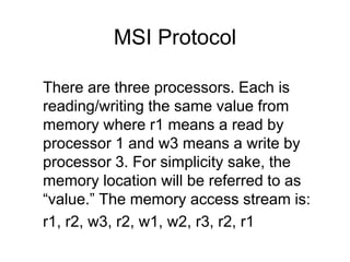
2. MSI Protocol
There are three processors. Each is
reading/writing the same value from
memory where r1 means a read by
processor 1 and w3 means a write by
processor 3. For simplicity sake, the
memory location will be referred to as
“value.” The memory access stream is:
r1, r2, w3, r2, w1, w2, r3, r2, r1
3. P1 P2 P3
Snooper Snooper Snooper
P1 wants to read the value. The cache does not
have itand generates a BusRd for the data. Main
memory controller provides the data. The data goes
into the cache in the shared state.
r1
PrRd
BusRd
value S
Main Memory
4. P1 P2 P3
PrRd
value S
Snooper Snooper Snooper
BusRd
r2
value S
Main Memory
P2 wants to read the value. Its cache does not have the
data, so it places a BusRd to notify other processors
and ask for the data. The memory controller provides
the data.
5. P1 P2 P3
value S
Snooper Snooper Snooper
w3
value S
P3 wants to write the value. It places a BusRdX to get
exclusive access and the most recent copy of the data.
The caches of P1 and P2 see the BusRdX and
invalidate their copies. Because the value is still up-to-date
in memory, memory provides the data.
PrWr
BusRdX
I I value M
Main Memory
6. P1 P2 P3
PrRd
S S
value I value M
Snooper Snooper Snooper
Flush
Main Memory
r2
value I
BusRd
P2 wants to read the value. P3’s cache has the most
up-to-date copy and will provide it. P2’s cache puts a
BusRd on the bus. P3’s cache snoops this and cancels
the memory access because it will provide the data.
P3’s cache flushes the data to the bus.
7. P1 P2 P3
PrWr
M I I
value I value S
Snooper Snooper Snooper
w1
value S
BusRdX
Main Memory
P1 wants to write to its cache. The cache places a
BusRdX on the bus to gain exclusive access and the
most up-to-date value. Main memory is not stale so it
provides the data. The snoopers for P2 and P3 see the
BusRdX and invalidate their copies in cache.
8. P1 P2 P3
PrWr
I M
value M value I
Snooper Snooper Snooper
w2
value I
BusRdX
Flush
Main Memory
P2 wants to write the value. Its cache places a BusRdX
to get exclusive access and the most recent copy of the
data. P1’s snooper sees the BusRdX and flushes the
data to the bus. Also, it invalides the data in its cache
and cancels the memory access.
9. P1 P2 P3
S S
value I value I
Snooper Snooper Snooper
Flush
Main Memory
r3
value M
PrRd
BusRd
P3 wants to read the value. Its cache does not have a
valid copy, so it places a BusRd on the bus. P2 has a
modified copy, so it flushes the data on the bus and
changes the status of the cache data to shared. The
flush cancels the memory accecss and updates the
data in memory as well.
10. P1 P2 P3
PrRd
value I value S
Snooper Snooper Snooper
r2
value S
Main Memory
P2 wants to read the value. Its cache has an up-to-date
copy. No bus transactions need to take place as there
is no cache miss.
11. P1 P2 P3
value I value S
Snooper Snooper Snooper
r1
value S
P1 wants to read the value. The cache does not have
it, so it places a BusRd onto the bus for the data. The
memory controller provides the data as it has an up-to-date
copy. The data goes into the cache in the shared
state.
PrRd
BusRd
S
Main Memory
12. MESI Protocol
There are three processors. Each is
loading or storing different words from
memory given as w0, w1, and w2.
These all map to the same location in
cache.
13. The memory accesses are as follows:
P1: ld w0, P3: ld w2
P1: st w0, P2: st w2
P2 st w2, P3 ld w0
P3: st w0
P1: ld w2
P2: ld w1
P3: ld w1
14. P1 P3
Snooper Snooper Snooper
P1 ld w0
P3 ld w2
In both loads, a cache miss happens so each cache
puts a BusRd onto the bus for the information. Main
memory is the owner and will provide the up-to-date
data. P1’s cache loads w0 in the E state. P3’s cache
loads w2 in the E state as well.
PrRd
BusRd(¬S)
PrRd
BusRd (¬S)
P2
w0 E w2 E
Main Memory
15. P1 P3
M w2 M I
w0 E w2 E
Snooper Snooper Snooper
P1 st w0
P2 st w2
P1 has w0 in the exclusive state, so on the cache hit, it does
not need to have a bus transaction. w2 is not in P2’s cache,
so the cache places a BusRdX to gain exclusive access.
Main memory provides the data because it is not stale even
though P3’s cache has the data. w2 is loaded in M state and
P3’s cache invalidates its copy of w2.
PrWr
Flush
P2
PrWr
BusRdX
Main Memory
16. P2 st w0
P3 ld w0 P2
P1 P3
PrWr PrRd
S w0 S
w0 M w2 M
w2 I
Snooper Snooper Snooper
BusRd(S) Flush
Main Memory
P2 executes another store to w2. It already has exclusive
access to w2 and the store results in a cache hit. No bus
transaction is issued by P2’s cache. P3 wants to load w0. This
results in a cache miss and the cache issues a BusRd
transaction. P1’s cache asserts the S signal because it has a
dirty w0 and provides the up-to-date data through a flush. P1
changes its state to S. P3’s cache loads w0 in the S state.
17. P1 P2
P3
I w2 M
w0 S w0 S
Snooper Snooper Snooper
P3 st w0
PrWr
M
Main Memory
P3 executes a store to w0. Both P1 and P3 have an up-to-date,
unmodified w0. What bus transactions are needed?
18. P1 P2
P3
w2 S
w0 S w2 M
w0 M
Snooper Snooper Snooper
Main Memory
P1 ld w2
P1 wants to load w2. P1’s cache does not have w2, so it issues
a BusRd transaction. P2’s cache turns on the S signal, so P1’s
cache knows to load w2 in the S state. P2’s cache provides w2
for P1 and cancels the access to main memory through a
Flush.
PrRd
BusRd(S)
S
Flush
19. P1 P2
P3
PrRd
w1 E
w2 S w2 S
w0 M
Snooper Snooper Snooper
P2 ld w1
BusRd(¬S)
Main Memory
P2 wants to load w1. This generates a cache miss. P2’s cache
issues a BusRd transaction. The S signal is not asserted, so it
knows that it has exclusive access to w1. Main memory
provides the data for w1. Should the state of w2 be changed in
P1 because it is the only cache that has a copy of w2?
20. P1 P2
P3
PrRd
S
w1 S
w2 S w1 E
w0 M
Snooper Snooper Snooper
P3 ld w1
BusRd(S)
Flush
Main Memory
P3 wants to load w1. This generates a cache miss. P3’s cache
issues a BusRd transaction. The S signal is asserted by P2’s
cache, so P3’s cache knows that it will load w1 in the S state.
Main memory provides the data for w1 because its copy is not
stale. P3 flushes w0 before loading w1.
Flush
21. Dragon Protocol
In this system there are 3 processors.
Each is loading or storing from memory
locations w0, w1, w2, and w3. w0 and
w1 are on the same cache line and are
loaded at the same time. Likewise for
w2 and w3. The two cache lines map to
the same location in cache.
22. P1 P3
Snooper Snooper Snooper
P1 ld w2
P1 wants to load w2. This generates a cache miss
and P1’s cache issues a BusRd bus transaction. The
S signal is not asserted, so the cache knows to load
w2 and w3 in the E state.
PrRd
BusRd(¬S)
P2
w2,w3 E
Main Memory
23. P1 P3
w2, w3 E
PrRd
P2
w0, w1 E
Snooper Snooper Snooper
BusRd(¬S)
P2 ld w0
Main Memory
P2 wants to load w0. This generates a cache miss
and P1’s cache issues a BusRd bus transaction. The
S signal is not asserted, so the cache knows to load
w0 and w1 in the E state.
24. P1 P3
w2, w3 E
P2
E
w0, w1 Sm
Sc
w0, w1
Snooper Snooper Snooper
PrWr
BusRd(S)
P3 st w1
BusUpd
Main Memory
Update
P3 wants to store w1. This generates a cache miss.
Memory will provide the data as no other cache has
this line in a modified state. After storing the new value
of w1, P3’s cache issues a BusUpd. P2 snoops this
and updates its cache with the updated w1.
25. P1 P2
P3
M
w2, w3 E w0, w1 Sc
w0, w1 Sm
Snooper Snooper Snooper
P1 st w3
PrRd
Main Memory
P1 issues store w3. It has exclusive access to this
cache line. What bus transactions does P1’s cache
issue?
26. P1 P2
P3
PrRd
Sm
w2, w3 M w2, w0, w1 w3
Sc
w0, w1 Sm
Snooper Snooper Snooper
P2 ld w3
BusRd(S)
???
Main Memory
Flush
P2 wants to load w3. This generates a cache miss. P2’s cache issues a
BusRd transaction. P1 asserts the S signal, so P2 will load the cache line
in Sc state. P1’s cache has a modified version of the cache line, so it will
provide the data for P2 with a flush transaction. P1’s cache will update the
line’s state to Sm. Should P3 change w0/w1’s state to M?
27. P2 ld w2
P3 st w0 P2
P1 P3
PrRd PrWr
w2, w3 Sm w2, w3 Sc
w0, w1 ?
Snooper Snooper Snooper
Main Memory
P2 wants to load w2. P3 wants to store w0. What are the
necessary bus transactions and cache updates that need to
take place?