際際滷

際際滷Share a Scribd company logo
JAWAHARLALNEHRU TECHNOLOGICALUNIVERSITY- GURAJADA-VIZIANAGARAM
VIZIANAGARAM  535 003Andhra Pradesh (India)
DESIGN AND VALIDATION OF MULTI-BAND
RECONFIGURABLE ANTENNA FOR WIRELESS APPLICATIONS
UNDER THE ESTEEMED
GUIDANCE OF :
Prof. K.Chandra Bhushana Rao
Professor of ECE
JNTU-GV
BATCH 5:
19VV1A0401 - A.J.Sridhar
19VV1A0424 - J.Sai Sri
19VV1A0427 - K.Hema Malini
19VV1A0452 - Shaik Mohammeed Abbas
19VV1A0455  S.Lochani Vilehya
CONTENTS:
 OBJECTIVE
 DESIGN PARAMETERS
 DESIGN EQUATIONS
 DESIGN AND VALIDATION PROCEDURE
 SIMULATION STEPS IN HFSS
 IMPLEMENTATION : 1. ANTENNA DESIGN STEPS
2. ANTENNA DESIGN
3. DESIGN PARAMETERS OF THE PATCH AND GROUND
4. PIN DIODE (BAR50-02V)
 PIN DIODE SWITCHING RESULTS
 CONCLUSION
STATUS REPORT
OBJECTIVE:
To design a Multi-band frequency reconfigurable antenna.
 Obtain results in terms of S parameter, E and H field patterns , 3-D gain plot , and
magnitude current distributions.
 To validate frequency reconfigurability of antenna with the help of switching of two
pin diodes.
DESIGN PARAMETERS:
1.S parameter : It describes how much the waves are reflected or transmitted from/ through a antenna.
The first parameter S11 is known as a reflection coefficient.
2. Resonant frequency : the frequency where maximum power is delivered to the patch of the antenna.
3.Gain : It is the ability of the antenna to radiate power more or less in any direction.
4.Directivity: the ratio of the radiation intensity in a given direction from the antenna to the radiation
intensity averaged over all directions.
5.Efficiency : It is the ratio of power radiated by the antenna to the power supplied to the antenna.
6.Front to back ratio: the ratio of power radiated in the front/main radiation lobe and the power radiated
in the opposite direction .
7.Impedance bandwidth: the range of frequencies where the antenna has good impedance matching and
can be heard by standing wave ratio (VSWR < 2) or module of the reflection coefficient (S11 <= -10 dB).
DESIGN EQUATIONS:
Empirical mathematical equations to
design square patch antenna are:
W =
Co
2
2
+1
, co is speed of light


= 0.412
+03


+0.264
0.258


+0.8
L =
Co
2fr 
-2
 In the typical design procedure of antenna,
three essential parameters are:
1. Resonance frequency fr
2. Dielectric constant of the substrate, 竜r
3. Thickness of substrate, h
 By increase in the substrate's dielectric constant
(竜r) and thickness (h) ,decreases the patch
dimensions and small changes in return loss,
bandwidth.
DESIGN AND VALIDATION PROCEDURE:
 Step-1: Synthesize the antenna dimensions based on the frequency of resonance, depending on the application.
 Step-2: Implement antenna design using simulation tool (HFSS).
 Step-3: Make the required changes to the antenna structure to get a multi-band operating response.
 Step-4: Include 2-pindiodes at appropriate places in the antenna structure.
 Step-5: Obtain the antenna design with 4 switching cases (ON-ON,ON-OFF,OFF-OFF,OFF-ON).
 Step-6: Optimize different parameters of the antenna to obtain optimal results.
 Step-7: Generate the resultant plots and values (S11,E and H plane Radiation pattern ,Gain , Directivity, Efficiency,
Front to Back Ratio , Current distribution ,Radiated power) to verify the performance of designed antenna at multiple
resonant frequency bands.
 Step-8: Fabricate the antenna and obtain the test results.
 Step-9: Compare the simulation results with the tested fabrication results.
 Step-10: Verify the antenna performance based on the comparison of simulation results with the tested fabrication
results.
SIMULATION STEPS IN HFSS:
1. Open HFSS insert HFSS design
2. Insert a substrate with required dimensions and assign FR4 epoxy material (=4.4)
3. Design the patch and ground structure on the same side of the substrate.
4. Assign the required boundaries to all parts of antenna .
5. Assign a lumped port to the feed line.
6. Insert the required radiation boundary such that it is 了/4 distance away from all outer surfaces
of the antenna.
7. Analyse and validate the antenna.
8. Obtain the resultant plots and values.
MINIMUM REQUIREMENTS OF PERFORMANCE PARAMETERS:
1. Return loss of antenna <= -10dB.
2. VSWR < 2.
3. Gain >= 3dB.
4. Radiation pattern of E and H field should be highly directional.
5. Radiation of antenna predominates in the Fresnels region ,which is the radiating near field of the antenna.
0.62
^3
了
< r <
2^2
了
d = maximum dimension of antenna
了 = wavelength
r = radius of the radiating sphere
6. In radiation pattern ,the major lobes must be predominant than the minor lobes.
IMPLEMENTATION:
ANTENNA DESIGN STEPS
STEP:1 STEP:2 STEP:3
STEP:4 STEP:5 STEP:6
STEP-1: Insert a box of length=35mm , width=40mm and height =1.6mm , which is defined as substrate.
STEP-2: Add a rectangle of with required dimensions, which is defined as ground.
STEP-3: Add 3 rectangles and unite them , to define a T shaped patch.
STEP-4: Add 2 more rectangles at required positions to create a slot.
STEP-5: Subtract the slots from the patch.
STEP-6: Insert two pin diodes in the slots.
STEP-7: Add a port to the T shaped patch.
STEP-8: Create a box inculcating antenna of dimensions larger than substate of antenna, which act as a radiation box.
STEP-9: Assign the required material, boundaries and excitation:
1. FR4 epoxy(竜 =4.4) - substate
2. perfect E boundary - patch and ground
3. lumped port - port
4. lumped RLC - switches
5. Radiation boundary and air medium - Radiation box
ANTENNA DESIGN
TOP VIEW 3D VIEW
patch
substrate
port
Ground
switch
Parameter Value(mm) Parameter Value(mm)
L1 40 W1 35
L2 36 W2 25
L3 19 W3 2.5
L4 2 W4 3.06
L5 3 g1 1
L6 2 g2 1
L7 2 G1 16
DESIGN PARAMETERS OF THE PATCH AND GROUND :
PIN-DIODE(BAR50-02V):
 In this project we used two PIN diodes.
 The design of the PIN diode is based on RLC excitation values.
 The diode is operated in OFF state where Lf = 0.6nH , Cp = 0.15pF and parallel resistance Rp = 5Kohm and when
operated in ON state , Lf = 0.6nH and series resistance Rs = 3 ohms.
 As we used 2 pin diodes , 4 switching cases are possible
state Cp Rp Lf Rs
ON - - 0.6 nH 3ohms
OFF 0.15pF 5Kohms 0.6 nH -
D1 D2
ON ON
ON OFF
OFF ON
OFF OFF
PIN-DIODE SWITCHINGRESULTS:
CONDITION RESONANT
FREQUENCY
IMPEDANCE
BANDWIDTH
ON-ON 1.8 GHz 353 MHz
ON-OFF 5.75 GHz
8.62 GHz
1.1133 GHz
390 MHz
OFF-OFF 6.21 GHz 1.3186 GHz
OFF-ON 2.48 GHz
5.14 GHZ
570 MHz
193.7 MHz
DIODE STATE RESONANT
FREQUENCY(GHz)
FREQUENCY
BAND
FH (GHz) FL (GHz) BANDWIDTH(FH-FL)
ON-ON 1.8 L 2.0119 1.6186 353 MHz
ON-OFF 5.75
8.62
C
X
6.51
8.86
5.3967
8.47
1.1133 GHz
390 MHz
OFF-ON 2.48
5.14
S
C
2.784
5.2337
2.212
5.04
570 MHz
193.7 MHz
OFF-OFF 6.21 C 7.21 5.8914 1.3186 GHz
BANDWIDTH CALCULATION:
 Draw a horizontal line on to S11 curve at -10dB, it cuts the deep of the resonant frequency curve at 2
points called FH(high frequency) and FL(low frequency)
 BANDWIDTH = High frequency  Low frequency (FH-FL)
E-Plane Radiation Pattern
D1,D2=ON,ON: AT RESONANT FREQUENCY = 1.8GHz
H-Plane Radiation Pattern
 Obtained two major lobes in both E and H field radiation patterns
E-field: 22.15V/m at 0deg and 23.32V/m at 180deg
H-field: 21.13A/m at 270deg and 21.07A/m at 90deg
Vector Current Distribution
3D-gain plot of antenna
E-field Distribution
Obtained a maximum gain of 5.6dB
D1,D2 = ON,OFF : AT RESONANT FREQUENCY = 5.75 GHz
E-Plane Radiation Pattern H-Plane Radiation Pattern
 Obtained two major lobes in both E and H field radiation patterns
E-field: 17.99V/m at 0deg and 18.32V/m at 180deg
H-field: 18.43A/m at 30deg , 18.01A/m at 135deg , 17.52A/m at 225deg , 18.37A/m at 330deg
Vector Current Distribution
3D-gain plot of antenna
E-field Distribution
Obtained a maximum gain of 1.98dB
D1,D2 = ON,OFF : AT RESONANT FREQUENCY = 8.62 GHz
E-Plane Radiation Pattern H-Plane Radiation Pattern
 Obtained major and minor lobes in both E and H field radiation patterns
E-field: 16.5V/m at 330deg , 14.73V/m at 10deg , 12.85V/m at 60deg , 13.08V/m at 120deg ,14.54V/m at 160deg,
14.46V/m at 240deg
H-field: 17.36A/m at 20deg , 17.82A/m at 90deg , 18.74A/m at 150deg , 17.33A/m at 225deg, 15.27A/m at 225deg
3D-gain plot of antenna
Vector Current Distribution
E-field Distribution
Obtained a maximum gain of 4.75dB
D1,D2 = OFF,ON : AT RESONANT FREQUENCY = 2.48 GHz
E-Plane Radiation Pattern H-Plane Radiation Pattern
 Obtained two major lobes in both E and H field radiation patterns
E-field: 20.3V/m at 0deg and 21.75V/m at 180deg
H-field: 19.02A/m at 90deg , 18.88A/m at 270deg
3D-gain plot of antenna
Vector Current Distribution
E-field Distribution
Obtained a maximum gain of 4.04dB
D1,D2 = OFF,ON : AT RESONANT FREQUENCY = 5.14 GHz
E-Plane Radiation Pattern H-Plane Radiation Pattern
 Obtained 2 major , 2 minor lobes in E field radiation pattern and 2 major lobes in H field radiation pattern
E-field: 11.41V/m at 60deg , 15.56V/m at 130deg , 19.47V/m at 220deg , 18.93V/m at 330deg.
H-field: 17.635A/m at 130deg , 17.63A/m at 220deg
3D-gain plot of antenna
Vector Current Distribution
E-field Distribution
Obtained a maximum gain of 2.014dB
D1,D2 = OFF,OFF : AT RESONANT FREQUENCY = 6.21 GHz
E-Plane Radiation Pattern H-Plane Radiation Pattern
 Obtained two major lobes in both E and H field radiation patterns
E-field: 13.01V/m at 60deg and 13.85V/m at 120deg,16.7V/m at 210deg , 18.75V/m at 340deg
H-field: 19.01A/m at 30deg , 19.09A/m at 130deg , 18.63A/m at 230deg , 18.99A/m at 330deg
3D-gain plot of antenna
Obtained a maximum gain of 2.89dB
Vector Current Distribution
E-field Distribution
REASONS FOR VARIATION OF THE RADIATION PATTERN IN 4 DIODE
SWITCHING CASES
 In general, the radiation pattern of an antenna is affected by a range of factors, including
1. the physical characteristics of the antenna
2. the frequency of the signal
3. By switching different elements using diodes
 In an antenna, diodes are often used as switches to switch different elements of the antenna on and off,
which can help to direct the radiation in a specific direction.
 When a diode is switched on or off, it can affect the current flowing through the antenna, and this can
affect the radiation pattern. Specifically, the diode switching can affect the phase and amplitude of the
electromagnetic waves radiated by the antenna.
 In a switchable beam antenna, when a diode is switched from a forward-biased state to a reverse-biased
state, the electric field within the diode can cause the charge carriers to be accelerated in the opposite
direction. This can result in the emission of radiation in a different direction than when the diode was in the
forward-biased state.
DIODE SWITCHING S11(REFLECTION
COEFFICIENT)
(dB)
IMPEDANCE
BANDWIDTH
RESONANT
FREQUENCY
(GHz)
FREQUENCY
BAND
GAIN
(dB)
DIRECTIVITY FRONT
BACK
RATIO
EFFICIEN
CY
RADIATED
POWER(W)
BAND
APPLICATIONS
ON ON -18.4457 353 MHz 1.8 GHz L 3.6324 2.24 1.3096 1.6216 1.5985 Bluetooth
ON OFF -38.2287
-13.3273
1.1133
GHz
390 MHz
5.75 GHz
8.62 GHz
C
X
1.5806
2.9854
1.8307
3.6549
1.9979
7.6014
0.8634
0.8168
0.8633
0.7788
WLAN
OFF OFF -29.0031 1.3186
GHz
6.21 GHz C 1.9467 2.1526 1.2347 0.9044 0.9941 WLAN
OFF ON -18.2855
-11.769
570 MHz
193.7
MHz
2.48 GHz
5.14 GHZ
S
C
2.5359
1.5903
2.5132
2.7222
1.394
6.0136
1.009
0.5842
0.5453
0.9032
Wi-Fi
WiMAX
ANTENNA WITH PIN DIODES RESULTS:
D1 D2
CONCLUSION:
 Measured results shows that the antenna exhibits frequency reconfigurability at four switching modes (ON-
ON,ON-OFF,OFF-ON,OFF-OFF) at six resonant frequencies 1.8GHz ,5.75GHz, 8.62GHz , 2.48GHz , 5.14GHz
and 6.21GHz.
 The antenna is operated at L,C,S and X band , exhibits almost omnidirectional radiation patterns both in E- and H-
planes.
 Due to the switching mechanism of the diode we obtained different radiation patterns in the 4 switching cases.
 The reflection coefficient (S11) is less than -10dB for all above frequencies which is a sign of better result.
 The gain obtained in the above frequencies are positive , it specifies the maximum input power is fed in a particular
direction.
 The resonant frequency range of antenna is used for the wireless applications like Bluetooth , WLAN, Wi-Fi and
WiMAX.
STATUS REPORT
WORK DONE:
 Antenna designing
 Analysed and verified antenna parameters
 Obtained frequency reconfigurability
 Obtained required plots and values through simulation in HFSS
WORK TO BE DONE:
 Antenna fabrication
Fabrication status : antenna structure is verified and will be fabricated within 10-15 days
 To obtain hardware results
 Comparison of hardware and simulation results
MULTIBAND reconfigurable antenna BATCH-5.pptx

More Related Content

Similar to MULTIBAND reconfigurable antenna BATCH-5.pptx (20)

Harmonic Suppression Dual-band Dipole Antenna with Parasitic Elements and a Stub
Harmonic Suppression Dual-band Dipole Antenna with Parasitic Elements and a StubHarmonic Suppression Dual-band Dipole Antenna with Parasitic Elements and a Stub
Harmonic Suppression Dual-band Dipole Antenna with Parasitic Elements and a Stub
TELKOMNIKA JOURNAL
M010327985
M010327985M010327985
M010327985
IOSR Journals
Antenna selection guide
Antenna selection guideAntenna selection guide
Antenna selection guide
D滴ng 畛
Ib3614041408
Ib3614041408Ib3614041408
Ib3614041408
IJERA Editor
Ib3614041408
Ib3614041408Ib3614041408
Ib3614041408
IJERA Editor
International Journal of Engineering and Science Invention (IJESI)
International Journal of Engineering and Science Invention (IJESI)International Journal of Engineering and Science Invention (IJESI)
International Journal of Engineering and Science Invention (IJESI)
inventionjournals
Microstrip patch antenna for pcs and wlan
Microstrip patch antenna for pcs and wlanMicrostrip patch antenna for pcs and wlan
Microstrip patch antenna for pcs and wlan
eSAT Journals
J010316368
J010316368J010316368
J010316368
IOSR Journals
A010510105
A010510105A010510105
A010510105
IOSR Journals
Research paper
Research paperResearch paper
Research paper
RESHMA MEENA
Design and Performance Enhancement of Vivaldi Antenna - Crimson Publishers
Design and Performance Enhancement of Vivaldi Antenna - Crimson PublishersDesign and Performance Enhancement of Vivaldi Antenna - Crimson Publishers
Design and Performance Enhancement of Vivaldi Antenna - Crimson Publishers
CrimsonPublishersRDMS
International Journal of Computational Engineering Research(IJCER)
International Journal of Computational Engineering Research(IJCER)International Journal of Computational Engineering Research(IJCER)
International Journal of Computational Engineering Research(IJCER)
ijceronline
FR1.T03.5 IGARSS_2011_Albers_22JUL2011.ppt
FR1.T03.5 IGARSS_2011_Albers_22JUL2011.pptFR1.T03.5 IGARSS_2011_Albers_22JUL2011.ppt
FR1.T03.5 IGARSS_2011_Albers_22JUL2011.ppt
grssieee
A bandwidth reconfigurable antenna for devices in low UWB-applications
A bandwidth reconfigurable antenna for devices in low UWB-applicationsA bandwidth reconfigurable antenna for devices in low UWB-applications
A bandwidth reconfigurable antenna for devices in low UWB-applications
TELKOMNIKA JOURNAL
SatCom_Numerical Probloms.pptx
SatCom_Numerical Probloms.pptxSatCom_Numerical Probloms.pptx
SatCom_Numerical Probloms.pptx
EshP1
Seminar
SeminarSeminar
Seminar
Sanket Yavalkar
A Slotted Elliptical Patch Antenna with a Shorting Pin for C-band Applications
A Slotted Elliptical Patch Antenna with a Shorting Pin for C-band ApplicationsA Slotted Elliptical Patch Antenna with a Shorting Pin for C-band Applications
A Slotted Elliptical Patch Antenna with a Shorting Pin for C-band Applications
IRJET Journal
Neksad patch antenna Project MobileTransisionP.pptx
Neksad patch antenna Project MobileTransisionP.pptxNeksad patch antenna Project MobileTransisionP.pptx
Neksad patch antenna Project MobileTransisionP.pptx
WilliamBlake55
Dual U-Slot Microstrip Patch Antenna with Enhanced Bandwidth
Dual U-Slot Microstrip Patch Antenna with Enhanced BandwidthDual U-Slot Microstrip Patch Antenna with Enhanced Bandwidth
Dual U-Slot Microstrip Patch Antenna with Enhanced Bandwidth
International Journal of Science and Research (IJSR)
A CPW-Fed Wideband And Multiband Rectangular Microstrip Patch Antenna For Wir...
A CPW-Fed Wideband And Multiband Rectangular Microstrip Patch Antenna For Wir...A CPW-Fed Wideband And Multiband Rectangular Microstrip Patch Antenna For Wir...
A CPW-Fed Wideband And Multiband Rectangular Microstrip Patch Antenna For Wir...
IJMER
Harmonic Suppression Dual-band Dipole Antenna with Parasitic Elements and a Stub
Harmonic Suppression Dual-band Dipole Antenna with Parasitic Elements and a StubHarmonic Suppression Dual-band Dipole Antenna with Parasitic Elements and a Stub
Harmonic Suppression Dual-band Dipole Antenna with Parasitic Elements and a Stub
TELKOMNIKA JOURNAL
Antenna selection guide
Antenna selection guideAntenna selection guide
Antenna selection guide
D滴ng 畛
International Journal of Engineering and Science Invention (IJESI)
International Journal of Engineering and Science Invention (IJESI)International Journal of Engineering and Science Invention (IJESI)
International Journal of Engineering and Science Invention (IJESI)
inventionjournals
Microstrip patch antenna for pcs and wlan
Microstrip patch antenna for pcs and wlanMicrostrip patch antenna for pcs and wlan
Microstrip patch antenna for pcs and wlan
eSAT Journals
Design and Performance Enhancement of Vivaldi Antenna - Crimson Publishers
Design and Performance Enhancement of Vivaldi Antenna - Crimson PublishersDesign and Performance Enhancement of Vivaldi Antenna - Crimson Publishers
Design and Performance Enhancement of Vivaldi Antenna - Crimson Publishers
CrimsonPublishersRDMS
International Journal of Computational Engineering Research(IJCER)
International Journal of Computational Engineering Research(IJCER)International Journal of Computational Engineering Research(IJCER)
International Journal of Computational Engineering Research(IJCER)
ijceronline
FR1.T03.5 IGARSS_2011_Albers_22JUL2011.ppt
FR1.T03.5 IGARSS_2011_Albers_22JUL2011.pptFR1.T03.5 IGARSS_2011_Albers_22JUL2011.ppt
FR1.T03.5 IGARSS_2011_Albers_22JUL2011.ppt
grssieee
A bandwidth reconfigurable antenna for devices in low UWB-applications
A bandwidth reconfigurable antenna for devices in low UWB-applicationsA bandwidth reconfigurable antenna for devices in low UWB-applications
A bandwidth reconfigurable antenna for devices in low UWB-applications
TELKOMNIKA JOURNAL
SatCom_Numerical Probloms.pptx
SatCom_Numerical Probloms.pptxSatCom_Numerical Probloms.pptx
SatCom_Numerical Probloms.pptx
EshP1
A Slotted Elliptical Patch Antenna with a Shorting Pin for C-band Applications
A Slotted Elliptical Patch Antenna with a Shorting Pin for C-band ApplicationsA Slotted Elliptical Patch Antenna with a Shorting Pin for C-band Applications
A Slotted Elliptical Patch Antenna with a Shorting Pin for C-band Applications
IRJET Journal
Neksad patch antenna Project MobileTransisionP.pptx
Neksad patch antenna Project MobileTransisionP.pptxNeksad patch antenna Project MobileTransisionP.pptx
Neksad patch antenna Project MobileTransisionP.pptx
WilliamBlake55
A CPW-Fed Wideband And Multiband Rectangular Microstrip Patch Antenna For Wir...
A CPW-Fed Wideband And Multiband Rectangular Microstrip Patch Antenna For Wir...A CPW-Fed Wideband And Multiband Rectangular Microstrip Patch Antenna For Wir...
A CPW-Fed Wideband And Multiband Rectangular Microstrip Patch Antenna For Wir...
IJMER

Recently uploaded (20)

Power Point Presentation for Electrical Engineering 3-phase.ppt
Power Point Presentation for Electrical Engineering 3-phase.pptPower Point Presentation for Electrical Engineering 3-phase.ppt
Power Point Presentation for Electrical Engineering 3-phase.ppt
Aniket_1415
Lecture -3 Cold water supply system.pptx
Lecture -3 Cold water supply system.pptxLecture -3 Cold water supply system.pptx
Lecture -3 Cold water supply system.pptx
rabiaatif2
Structural QA/QC Inspection in KRP 401600 | Copper Processing Plant-3 (MOF-3)...
Structural QA/QC Inspection in KRP 401600 | Copper Processing Plant-3 (MOF-3)...Structural QA/QC Inspection in KRP 401600 | Copper Processing Plant-3 (MOF-3)...
Structural QA/QC Inspection in KRP 401600 | Copper Processing Plant-3 (MOF-3)...
slayshadow705
US Patented ReGenX Generator, ReGen-X Quatum Motor EV Regenerative Accelerati...
US Patented ReGenX Generator, ReGen-X Quatum Motor EV Regenerative Accelerati...US Patented ReGenX Generator, ReGen-X Quatum Motor EV Regenerative Accelerati...
US Patented ReGenX Generator, ReGen-X Quatum Motor EV Regenerative Accelerati...
Thane Heins NOBEL PRIZE WINNING ENERGY RESEARCHER
eng funda notes.pdfddddddddddddddddddddddd
eng funda notes.pdfdddddddddddddddddddddddeng funda notes.pdfddddddddddddddddddddddd
eng funda notes.pdfddddddddddddddddddddddd
aayushkumarsinghec22
How to Make an RFID Door Lock System using Arduino
How to Make an RFID Door Lock System using ArduinoHow to Make an RFID Door Lock System using Arduino
How to Make an RFID Door Lock System using Arduino
CircuitDigest
Name.docxVVVVVVVVVVVVVVVVVVVVVVVVVVVVVVVVVVVVVVVVVVVV
Name.docxVVVVVVVVVVVVVVVVVVVVVVVVVVVVVVVVVVVVVVVVVVVVName.docxVVVVVVVVVVVVVVVVVVVVVVVVVVVVVVVVVVVVVVVVVVVV
Name.docxVVVVVVVVVVVVVVVVVVVVVVVVVVVVVVVVVVVVVVVVVVVV
MerijimArsedelPalmad1
Equipment for Gas Metal Arc Welding Process
Equipment for Gas Metal Arc Welding ProcessEquipment for Gas Metal Arc Welding Process
Equipment for Gas Metal Arc Welding Process
AhmadKamil87
CONTRACTOR ALL RISK INSURANCESAR (1).ppt
CONTRACTOR ALL RISK INSURANCESAR (1).pptCONTRACTOR ALL RISK INSURANCESAR (1).ppt
CONTRACTOR ALL RISK INSURANCESAR (1).ppt
suaktonny
Indian Soil Classification System in Geotechnical Engineering
Indian Soil Classification System in Geotechnical EngineeringIndian Soil Classification System in Geotechnical Engineering
Indian Soil Classification System in Geotechnical Engineering
Rajani Vyawahare
Env and Water Supply Engg._Dr. Hasan.pdf
Env and Water Supply Engg._Dr. Hasan.pdfEnv and Water Supply Engg._Dr. Hasan.pdf
Env and Water Supply Engg._Dr. Hasan.pdf
MahmudHasan747870
Industrial Valves, Instruments Products Profile
Industrial Valves, Instruments Products ProfileIndustrial Valves, Instruments Products Profile
Industrial Valves, Instruments Products Profile
zebcoeng
UNIT 1FUNDAMENTALS OF OPERATING SYSTEMS.pptx
UNIT 1FUNDAMENTALS OF OPERATING SYSTEMS.pptxUNIT 1FUNDAMENTALS OF OPERATING SYSTEMS.pptx
UNIT 1FUNDAMENTALS OF OPERATING SYSTEMS.pptx
KesavanT10
Mathematics_behind_machine_learning_INT255.pptx
Mathematics_behind_machine_learning_INT255.pptxMathematics_behind_machine_learning_INT255.pptx
Mathematics_behind_machine_learning_INT255.pptx
ppkmurthy2006
Best KNow Hydrogen Fuel Production in the World The cost in USD kwh for H2
Best KNow  Hydrogen Fuel Production in the World The cost in USD kwh for H2Best KNow  Hydrogen Fuel Production in the World The cost in USD kwh for H2
Best KNow Hydrogen Fuel Production in the World The cost in USD kwh for H2
Daniel Donatelli
Piping-and-pipeline-calculations-manual.pdf
Piping-and-pipeline-calculations-manual.pdfPiping-and-pipeline-calculations-manual.pdf
Piping-and-pipeline-calculations-manual.pdf
OMI0721
G8 mini project for alcohol detection and engine lock system with GPS tracki...
G8 mini project for  alcohol detection and engine lock system with GPS tracki...G8 mini project for  alcohol detection and engine lock system with GPS tracki...
G8 mini project for alcohol detection and engine lock system with GPS tracki...
sahillanjewar294
Frankfurt University of Applied Science urkunde
Frankfurt University of Applied Science urkundeFrankfurt University of Applied Science urkunde
Frankfurt University of Applied Science urkunde
Lisa Emerson
15. Smart Cities Big Data, Civic Hackers, and the Quest for a New Utopia.pdf
15. Smart Cities Big Data, Civic Hackers, and the Quest for a New Utopia.pdf15. Smart Cities Big Data, Civic Hackers, and the Quest for a New Utopia.pdf
15. Smart Cities Big Data, Civic Hackers, and the Quest for a New Utopia.pdf
NgocThang9
Water Industry Process Automation & Control Monthly - March 2025.pdf
Water Industry Process Automation & Control Monthly - March 2025.pdfWater Industry Process Automation & Control Monthly - March 2025.pdf
Water Industry Process Automation & Control Monthly - March 2025.pdf
Water Industry Process Automation & Control
Power Point Presentation for Electrical Engineering 3-phase.ppt
Power Point Presentation for Electrical Engineering 3-phase.pptPower Point Presentation for Electrical Engineering 3-phase.ppt
Power Point Presentation for Electrical Engineering 3-phase.ppt
Aniket_1415
Lecture -3 Cold water supply system.pptx
Lecture -3 Cold water supply system.pptxLecture -3 Cold water supply system.pptx
Lecture -3 Cold water supply system.pptx
rabiaatif2
Structural QA/QC Inspection in KRP 401600 | Copper Processing Plant-3 (MOF-3)...
Structural QA/QC Inspection in KRP 401600 | Copper Processing Plant-3 (MOF-3)...Structural QA/QC Inspection in KRP 401600 | Copper Processing Plant-3 (MOF-3)...
Structural QA/QC Inspection in KRP 401600 | Copper Processing Plant-3 (MOF-3)...
slayshadow705
eng funda notes.pdfddddddddddddddddddddddd
eng funda notes.pdfdddddddddddddddddddddddeng funda notes.pdfddddddddddddddddddddddd
eng funda notes.pdfddddddddddddddddddddddd
aayushkumarsinghec22
How to Make an RFID Door Lock System using Arduino
How to Make an RFID Door Lock System using ArduinoHow to Make an RFID Door Lock System using Arduino
How to Make an RFID Door Lock System using Arduino
CircuitDigest
Name.docxVVVVVVVVVVVVVVVVVVVVVVVVVVVVVVVVVVVVVVVVVVVV
Name.docxVVVVVVVVVVVVVVVVVVVVVVVVVVVVVVVVVVVVVVVVVVVVName.docxVVVVVVVVVVVVVVVVVVVVVVVVVVVVVVVVVVVVVVVVVVVV
Name.docxVVVVVVVVVVVVVVVVVVVVVVVVVVVVVVVVVVVVVVVVVVVV
MerijimArsedelPalmad1
Equipment for Gas Metal Arc Welding Process
Equipment for Gas Metal Arc Welding ProcessEquipment for Gas Metal Arc Welding Process
Equipment for Gas Metal Arc Welding Process
AhmadKamil87
CONTRACTOR ALL RISK INSURANCESAR (1).ppt
CONTRACTOR ALL RISK INSURANCESAR (1).pptCONTRACTOR ALL RISK INSURANCESAR (1).ppt
CONTRACTOR ALL RISK INSURANCESAR (1).ppt
suaktonny
Indian Soil Classification System in Geotechnical Engineering
Indian Soil Classification System in Geotechnical EngineeringIndian Soil Classification System in Geotechnical Engineering
Indian Soil Classification System in Geotechnical Engineering
Rajani Vyawahare
Env and Water Supply Engg._Dr. Hasan.pdf
Env and Water Supply Engg._Dr. Hasan.pdfEnv and Water Supply Engg._Dr. Hasan.pdf
Env and Water Supply Engg._Dr. Hasan.pdf
MahmudHasan747870
Industrial Valves, Instruments Products Profile
Industrial Valves, Instruments Products ProfileIndustrial Valves, Instruments Products Profile
Industrial Valves, Instruments Products Profile
zebcoeng
UNIT 1FUNDAMENTALS OF OPERATING SYSTEMS.pptx
UNIT 1FUNDAMENTALS OF OPERATING SYSTEMS.pptxUNIT 1FUNDAMENTALS OF OPERATING SYSTEMS.pptx
UNIT 1FUNDAMENTALS OF OPERATING SYSTEMS.pptx
KesavanT10
Mathematics_behind_machine_learning_INT255.pptx
Mathematics_behind_machine_learning_INT255.pptxMathematics_behind_machine_learning_INT255.pptx
Mathematics_behind_machine_learning_INT255.pptx
ppkmurthy2006
Best KNow Hydrogen Fuel Production in the World The cost in USD kwh for H2
Best KNow  Hydrogen Fuel Production in the World The cost in USD kwh for H2Best KNow  Hydrogen Fuel Production in the World The cost in USD kwh for H2
Best KNow Hydrogen Fuel Production in the World The cost in USD kwh for H2
Daniel Donatelli
Piping-and-pipeline-calculations-manual.pdf
Piping-and-pipeline-calculations-manual.pdfPiping-and-pipeline-calculations-manual.pdf
Piping-and-pipeline-calculations-manual.pdf
OMI0721
G8 mini project for alcohol detection and engine lock system with GPS tracki...
G8 mini project for  alcohol detection and engine lock system with GPS tracki...G8 mini project for  alcohol detection and engine lock system with GPS tracki...
G8 mini project for alcohol detection and engine lock system with GPS tracki...
sahillanjewar294
Frankfurt University of Applied Science urkunde
Frankfurt University of Applied Science urkundeFrankfurt University of Applied Science urkunde
Frankfurt University of Applied Science urkunde
Lisa Emerson
15. Smart Cities Big Data, Civic Hackers, and the Quest for a New Utopia.pdf
15. Smart Cities Big Data, Civic Hackers, and the Quest for a New Utopia.pdf15. Smart Cities Big Data, Civic Hackers, and the Quest for a New Utopia.pdf
15. Smart Cities Big Data, Civic Hackers, and the Quest for a New Utopia.pdf
NgocThang9

MULTIBAND reconfigurable antenna BATCH-5.pptx

  • 1. JAWAHARLALNEHRU TECHNOLOGICALUNIVERSITY- GURAJADA-VIZIANAGARAM VIZIANAGARAM 535 003Andhra Pradesh (India) DESIGN AND VALIDATION OF MULTI-BAND RECONFIGURABLE ANTENNA FOR WIRELESS APPLICATIONS UNDER THE ESTEEMED GUIDANCE OF : Prof. K.Chandra Bhushana Rao Professor of ECE JNTU-GV BATCH 5: 19VV1A0401 - A.J.Sridhar 19VV1A0424 - J.Sai Sri 19VV1A0427 - K.Hema Malini 19VV1A0452 - Shaik Mohammeed Abbas 19VV1A0455 S.Lochani Vilehya
  • 2. CONTENTS: OBJECTIVE DESIGN PARAMETERS DESIGN EQUATIONS DESIGN AND VALIDATION PROCEDURE SIMULATION STEPS IN HFSS IMPLEMENTATION : 1. ANTENNA DESIGN STEPS 2. ANTENNA DESIGN 3. DESIGN PARAMETERS OF THE PATCH AND GROUND 4. PIN DIODE (BAR50-02V) PIN DIODE SWITCHING RESULTS CONCLUSION STATUS REPORT
  • 3. OBJECTIVE: To design a Multi-band frequency reconfigurable antenna. Obtain results in terms of S parameter, E and H field patterns , 3-D gain plot , and magnitude current distributions. To validate frequency reconfigurability of antenna with the help of switching of two pin diodes.
  • 4. DESIGN PARAMETERS: 1.S parameter : It describes how much the waves are reflected or transmitted from/ through a antenna. The first parameter S11 is known as a reflection coefficient. 2. Resonant frequency : the frequency where maximum power is delivered to the patch of the antenna. 3.Gain : It is the ability of the antenna to radiate power more or less in any direction. 4.Directivity: the ratio of the radiation intensity in a given direction from the antenna to the radiation intensity averaged over all directions. 5.Efficiency : It is the ratio of power radiated by the antenna to the power supplied to the antenna. 6.Front to back ratio: the ratio of power radiated in the front/main radiation lobe and the power radiated in the opposite direction . 7.Impedance bandwidth: the range of frequencies where the antenna has good impedance matching and can be heard by standing wave ratio (VSWR < 2) or module of the reflection coefficient (S11 <= -10 dB).
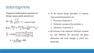
  • 5. DESIGN EQUATIONS: Empirical mathematical equations to design square patch antenna are: W = Co 2 2 +1 , co is speed of light = 0.412 +03 +0.264 0.258 +0.8 L = Co 2fr -2 In the typical design procedure of antenna, three essential parameters are: 1. Resonance frequency fr 2. Dielectric constant of the substrate, 竜r 3. Thickness of substrate, h By increase in the substrate's dielectric constant (竜r) and thickness (h) ,decreases the patch dimensions and small changes in return loss, bandwidth.
  • 6. DESIGN AND VALIDATION PROCEDURE: Step-1: Synthesize the antenna dimensions based on the frequency of resonance, depending on the application. Step-2: Implement antenna design using simulation tool (HFSS). Step-3: Make the required changes to the antenna structure to get a multi-band operating response. Step-4: Include 2-pindiodes at appropriate places in the antenna structure. Step-5: Obtain the antenna design with 4 switching cases (ON-ON,ON-OFF,OFF-OFF,OFF-ON). Step-6: Optimize different parameters of the antenna to obtain optimal results. Step-7: Generate the resultant plots and values (S11,E and H plane Radiation pattern ,Gain , Directivity, Efficiency, Front to Back Ratio , Current distribution ,Radiated power) to verify the performance of designed antenna at multiple resonant frequency bands. Step-8: Fabricate the antenna and obtain the test results. Step-9: Compare the simulation results with the tested fabrication results. Step-10: Verify the antenna performance based on the comparison of simulation results with the tested fabrication results.
  • 7. SIMULATION STEPS IN HFSS: 1. Open HFSS insert HFSS design 2. Insert a substrate with required dimensions and assign FR4 epoxy material (=4.4) 3. Design the patch and ground structure on the same side of the substrate. 4. Assign the required boundaries to all parts of antenna . 5. Assign a lumped port to the feed line. 6. Insert the required radiation boundary such that it is 了/4 distance away from all outer surfaces of the antenna. 7. Analyse and validate the antenna. 8. Obtain the resultant plots and values.
  • 8. MINIMUM REQUIREMENTS OF PERFORMANCE PARAMETERS: 1. Return loss of antenna <= -10dB. 2. VSWR < 2. 3. Gain >= 3dB. 4. Radiation pattern of E and H field should be highly directional. 5. Radiation of antenna predominates in the Fresnels region ,which is the radiating near field of the antenna. 0.62 ^3 了 < r < 2^2 了 d = maximum dimension of antenna 了 = wavelength r = radius of the radiating sphere 6. In radiation pattern ,the major lobes must be predominant than the minor lobes.
  • 9. IMPLEMENTATION: ANTENNA DESIGN STEPS STEP:1 STEP:2 STEP:3 STEP:4 STEP:5 STEP:6
  • 10. STEP-1: Insert a box of length=35mm , width=40mm and height =1.6mm , which is defined as substrate. STEP-2: Add a rectangle of with required dimensions, which is defined as ground. STEP-3: Add 3 rectangles and unite them , to define a T shaped patch. STEP-4: Add 2 more rectangles at required positions to create a slot. STEP-5: Subtract the slots from the patch. STEP-6: Insert two pin diodes in the slots. STEP-7: Add a port to the T shaped patch. STEP-8: Create a box inculcating antenna of dimensions larger than substate of antenna, which act as a radiation box. STEP-9: Assign the required material, boundaries and excitation: 1. FR4 epoxy(竜 =4.4) - substate 2. perfect E boundary - patch and ground 3. lumped port - port 4. lumped RLC - switches 5. Radiation boundary and air medium - Radiation box
  • 11. ANTENNA DESIGN TOP VIEW 3D VIEW patch substrate port Ground switch
  • 12. Parameter Value(mm) Parameter Value(mm) L1 40 W1 35 L2 36 W2 25 L3 19 W3 2.5 L4 2 W4 3.06 L5 3 g1 1 L6 2 g2 1 L7 2 G1 16 DESIGN PARAMETERS OF THE PATCH AND GROUND :
  • 13. PIN-DIODE(BAR50-02V): In this project we used two PIN diodes. The design of the PIN diode is based on RLC excitation values. The diode is operated in OFF state where Lf = 0.6nH , Cp = 0.15pF and parallel resistance Rp = 5Kohm and when operated in ON state , Lf = 0.6nH and series resistance Rs = 3 ohms. As we used 2 pin diodes , 4 switching cases are possible state Cp Rp Lf Rs ON - - 0.6 nH 3ohms OFF 0.15pF 5Kohms 0.6 nH - D1 D2 ON ON ON OFF OFF ON OFF OFF
  • 14. PIN-DIODE SWITCHINGRESULTS: CONDITION RESONANT FREQUENCY IMPEDANCE BANDWIDTH ON-ON 1.8 GHz 353 MHz ON-OFF 5.75 GHz 8.62 GHz 1.1133 GHz 390 MHz OFF-OFF 6.21 GHz 1.3186 GHz OFF-ON 2.48 GHz 5.14 GHZ 570 MHz 193.7 MHz
  • 15. DIODE STATE RESONANT FREQUENCY(GHz) FREQUENCY BAND FH (GHz) FL (GHz) BANDWIDTH(FH-FL) ON-ON 1.8 L 2.0119 1.6186 353 MHz ON-OFF 5.75 8.62 C X 6.51 8.86 5.3967 8.47 1.1133 GHz 390 MHz OFF-ON 2.48 5.14 S C 2.784 5.2337 2.212 5.04 570 MHz 193.7 MHz OFF-OFF 6.21 C 7.21 5.8914 1.3186 GHz BANDWIDTH CALCULATION: Draw a horizontal line on to S11 curve at -10dB, it cuts the deep of the resonant frequency curve at 2 points called FH(high frequency) and FL(low frequency) BANDWIDTH = High frequency Low frequency (FH-FL)
  • 16. E-Plane Radiation Pattern D1,D2=ON,ON: AT RESONANT FREQUENCY = 1.8GHz H-Plane Radiation Pattern Obtained two major lobes in both E and H field radiation patterns E-field: 22.15V/m at 0deg and 23.32V/m at 180deg H-field: 21.13A/m at 270deg and 21.07A/m at 90deg
  • 17. Vector Current Distribution 3D-gain plot of antenna E-field Distribution Obtained a maximum gain of 5.6dB
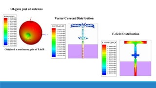
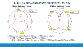
  • 18. D1,D2 = ON,OFF : AT RESONANT FREQUENCY = 5.75 GHz E-Plane Radiation Pattern H-Plane Radiation Pattern Obtained two major lobes in both E and H field radiation patterns E-field: 17.99V/m at 0deg and 18.32V/m at 180deg H-field: 18.43A/m at 30deg , 18.01A/m at 135deg , 17.52A/m at 225deg , 18.37A/m at 330deg
  • 19. Vector Current Distribution 3D-gain plot of antenna E-field Distribution Obtained a maximum gain of 1.98dB
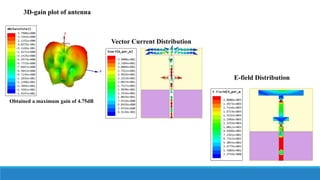
  • 20. D1,D2 = ON,OFF : AT RESONANT FREQUENCY = 8.62 GHz E-Plane Radiation Pattern H-Plane Radiation Pattern Obtained major and minor lobes in both E and H field radiation patterns E-field: 16.5V/m at 330deg , 14.73V/m at 10deg , 12.85V/m at 60deg , 13.08V/m at 120deg ,14.54V/m at 160deg, 14.46V/m at 240deg H-field: 17.36A/m at 20deg , 17.82A/m at 90deg , 18.74A/m at 150deg , 17.33A/m at 225deg, 15.27A/m at 225deg
  • 21. 3D-gain plot of antenna Vector Current Distribution E-field Distribution Obtained a maximum gain of 4.75dB
  • 22. D1,D2 = OFF,ON : AT RESONANT FREQUENCY = 2.48 GHz E-Plane Radiation Pattern H-Plane Radiation Pattern Obtained two major lobes in both E and H field radiation patterns E-field: 20.3V/m at 0deg and 21.75V/m at 180deg H-field: 19.02A/m at 90deg , 18.88A/m at 270deg
  • 23. 3D-gain plot of antenna Vector Current Distribution E-field Distribution Obtained a maximum gain of 4.04dB
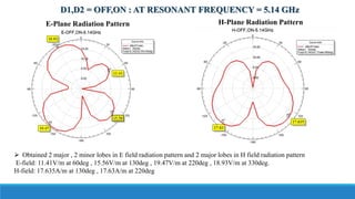
  • 24. D1,D2 = OFF,ON : AT RESONANT FREQUENCY = 5.14 GHz E-Plane Radiation Pattern H-Plane Radiation Pattern Obtained 2 major , 2 minor lobes in E field radiation pattern and 2 major lobes in H field radiation pattern E-field: 11.41V/m at 60deg , 15.56V/m at 130deg , 19.47V/m at 220deg , 18.93V/m at 330deg. H-field: 17.635A/m at 130deg , 17.63A/m at 220deg
  • 25. 3D-gain plot of antenna Vector Current Distribution E-field Distribution Obtained a maximum gain of 2.014dB
  • 26. D1,D2 = OFF,OFF : AT RESONANT FREQUENCY = 6.21 GHz E-Plane Radiation Pattern H-Plane Radiation Pattern Obtained two major lobes in both E and H field radiation patterns E-field: 13.01V/m at 60deg and 13.85V/m at 120deg,16.7V/m at 210deg , 18.75V/m at 340deg H-field: 19.01A/m at 30deg , 19.09A/m at 130deg , 18.63A/m at 230deg , 18.99A/m at 330deg
  • 27. 3D-gain plot of antenna Obtained a maximum gain of 2.89dB Vector Current Distribution E-field Distribution
  • 28. REASONS FOR VARIATION OF THE RADIATION PATTERN IN 4 DIODE SWITCHING CASES In general, the radiation pattern of an antenna is affected by a range of factors, including 1. the physical characteristics of the antenna 2. the frequency of the signal 3. By switching different elements using diodes In an antenna, diodes are often used as switches to switch different elements of the antenna on and off, which can help to direct the radiation in a specific direction. When a diode is switched on or off, it can affect the current flowing through the antenna, and this can affect the radiation pattern. Specifically, the diode switching can affect the phase and amplitude of the electromagnetic waves radiated by the antenna. In a switchable beam antenna, when a diode is switched from a forward-biased state to a reverse-biased state, the electric field within the diode can cause the charge carriers to be accelerated in the opposite direction. This can result in the emission of radiation in a different direction than when the diode was in the forward-biased state.
  • 29. DIODE SWITCHING S11(REFLECTION COEFFICIENT) (dB) IMPEDANCE BANDWIDTH RESONANT FREQUENCY (GHz) FREQUENCY BAND GAIN (dB) DIRECTIVITY FRONT BACK RATIO EFFICIEN CY RADIATED POWER(W) BAND APPLICATIONS ON ON -18.4457 353 MHz 1.8 GHz L 3.6324 2.24 1.3096 1.6216 1.5985 Bluetooth ON OFF -38.2287 -13.3273 1.1133 GHz 390 MHz 5.75 GHz 8.62 GHz C X 1.5806 2.9854 1.8307 3.6549 1.9979 7.6014 0.8634 0.8168 0.8633 0.7788 WLAN OFF OFF -29.0031 1.3186 GHz 6.21 GHz C 1.9467 2.1526 1.2347 0.9044 0.9941 WLAN OFF ON -18.2855 -11.769 570 MHz 193.7 MHz 2.48 GHz 5.14 GHZ S C 2.5359 1.5903 2.5132 2.7222 1.394 6.0136 1.009 0.5842 0.5453 0.9032 Wi-Fi WiMAX ANTENNA WITH PIN DIODES RESULTS: D1 D2
  • 30. CONCLUSION: Measured results shows that the antenna exhibits frequency reconfigurability at four switching modes (ON- ON,ON-OFF,OFF-ON,OFF-OFF) at six resonant frequencies 1.8GHz ,5.75GHz, 8.62GHz , 2.48GHz , 5.14GHz and 6.21GHz. The antenna is operated at L,C,S and X band , exhibits almost omnidirectional radiation patterns both in E- and H- planes. Due to the switching mechanism of the diode we obtained different radiation patterns in the 4 switching cases. The reflection coefficient (S11) is less than -10dB for all above frequencies which is a sign of better result. The gain obtained in the above frequencies are positive , it specifies the maximum input power is fed in a particular direction. The resonant frequency range of antenna is used for the wireless applications like Bluetooth , WLAN, Wi-Fi and WiMAX.
  • 31. STATUS REPORT WORK DONE: Antenna designing Analysed and verified antenna parameters Obtained frequency reconfigurability Obtained required plots and values through simulation in HFSS WORK TO BE DONE: Antenna fabrication Fabrication status : antenna structure is verified and will be fabricated within 10-15 days To obtain hardware results Comparison of hardware and simulation results