際際滷

際際滷Share a Scribd company logo
PCB Design and Fabrication
Content
1. Prepare your circuit artwork.
2. Exposing
3. Developing
4. Trouble shooting
5. Etching
Prepare your circuit artwork
1. We need a schematic diagram
i. Design by ourselves
ii. Readymade (Internet, datasheet etc)
Eg. https://www.arduino.cc/en/Main/ArduinoBoardUno
2. What should we have on the schematic?
i. Circuit diagram.
ii. Name of the part used.
3. Software to design PCB
i. Eagle (http://www.cadsoftusa.com/)
ii. Proteus(http://www.labcenter.com/products/pcb/schematic_intro.cfm)
iii. Pads (https://www.pads.com/)
1
PCB Design Tutorial using Eagle Software
 Installing
 Download trial from http://www.cadsoftusa.com/download-eagle/
1 Prepare your circuit artwork
Create new project
>File > New >Project
A new project folder is made under
the project. Set the name of the
project folder by renaming.
When the project is working, it isn't
possible to change the name. In this
case, select "Close Project" from the
menu. When a project is closed, the
green mark changes to the small
gray mark.
1
Starting a New Project
Prepare your circuit artwork
The file to draw a schematic must
be made after creating a project.
Select "New" from the menu which
is displayed by right clicking the
project and select "Schematic".
By above operation, the window
to draw a schematic is displayed
newly.
In this condition, an actual file isn't
made yet.
1
Create Schematic File
Prepare your circuit artwork
Select File menu and select "Save as...". The file is made with this
operation.
Write the name of the schematic.
A file of .sch is saved by pushing the Save button.
1
Create Schematic File
Prepare your circuit artwork
1
Create Board File
Prepare your circuit artwork
In the project, another important file must be createdcalled the board
to draw the mask pattern for the printed board. The board file can be
created after drawing a schematic. When adding a part to the
schematic, a part is added to the board, too. So, when drawing a
schematic, it is necessary to keep a board file always open condition.
Click "Board" icon in the schematic window
When a board isn't made yet,
board creating is confirmed by
following dialog.
1
Create Board File
Prepare your circuit artwork
Following board window is displayed. In this condition, an actual file isn't
made yet.
A board file is made by clicking "Save" icon in the board window.
The file name is same as the schematic file. But, the extension is ".brd"
1
Schematic and Board File Created
Prepare your circuit artwork
The existence of the schematic file and the board file can be confirmed by
the project folder of the control panel.
The working environment was ready with above operations.
1
Selecting and Adding Parts
Prepare your circuit artwork
To make the mask pattern of the printed board, the schematic must be
drawn. The part which is used with the schematic is chosen from the
one which is registered on the library.
Click the "ADD" button which is put on the left side in the
schematic window. NOTE: this screen is displayed
when the use status is active,
marked by green bullet. Right
click the Library folder and click
Use All.
1
Selecting and Adding Parts
Prepare your circuit artwork
When pushing the OK button, a
part is displayed on the
schematic. Push the left button
of the mouse in the position.
Click one more to get another
same part.
To stop the addition function of the
part, push an ESC key and "Cancel"
button in the schematic window
1
Wiring Parts
Prepare your circuit artwork
After we put the component, then wiring can be
done by the Wire function. Left click the lead wire
of the part and double-click at the end point which
of wiring. It isn't necessary to keep to push the
mouse button during wiring work. To stop this
feature, press STOP button.
The drawn line can be erased using
the Delete button.
1
Exercise!
Prepare your circuit artwork
Draw this circuit now!.. A 5 volt voltage regulator circuit.
After drawing a schematic, the mistake can be
automatically detected by the ERC (Electrical Rule Check)
button.
1
Exercise!
Prepare your circuit artwork
Part Value Package Library Units
D1 - D4
1N4148DO35-
7 DO35-7 diode 4
K1 - K4 G5V-2 G5V-2 relay 4
LED1 -
LED4 LED3MM led 4
Rx 1k 0207/7 rcl 8
Rx 10k 0207/7 rcl 4
T1 - T4 2N3904 TO92 transistor 4
VS-6V VS-6V 22-23-2021 con-molex 1
VS-6V1 VS-6V 22-23-2021 con-molex 1
X1 22-23-2041 22-23-2041 con-molex 1
X2 22-23-2041 22-23-2041 con-molex 1
MOTOA MOTOA 22-23-2021 con-molex 1
MOTOB MOTOB 22-23-2021 con-molex 1
Part List
1
Creating Board file
Prepare your circuit artwork
When the schematic drawing is ready, click Board button from schematic file.
The yellow line among the parts is the line which shows a connection among the
parts. But, these lines are not wiring for the printed board yet.
1
Parts arrangement on the board
Prepare your circuit artwork
The parts of the board are arranged out of the printed board. After pushing the
Move button, move the parts inside the frame. We can also put text inside.
The yellow line shows a connection among the parts.
The part should be arranged for the yellow line to be simpler.
1
Autorouting on the board
Prepare your circuit artwork
Automatically wiring is done by the "Auto" button.

More Related Content

What's hot (20)

Workshop on pcb
Workshop on pcbWorkshop on pcb
Workshop on pcb
Mahmudur Rana
PCB
PCBPCB
PCB
SUneel Gupta
PCB DESIGN - Introduction to PCB Design Library Creation
PCB DESIGN -  Introduction to PCB Design Library Creation PCB DESIGN -  Introduction to PCB Design Library Creation
PCB DESIGN - Introduction to PCB Design Library Creation
Vibrant Technologies & Computers
Designing process of printed circuit boards
Designing process of printed circuit boardsDesigning process of printed circuit boards
Designing process of printed circuit boards
elprocus
PCB Designing
PCB Designing PCB Designing
PCB Designing
Anant Prakashrakash Verma
PPT ON PCB DESIGN INTERNSHIP
PPT ON PCB DESIGN INTERNSHIPPPT ON PCB DESIGN INTERNSHIP
PPT ON PCB DESIGN INTERNSHIP
SujoyHalder4
How To Design PCB
How To Design PCBHow To Design PCB
How To Design PCB
Sharan kumar
Printed board circuit design (Pcb) PPT
 Printed board circuit design (Pcb) PPT Printed board circuit design (Pcb) PPT
Printed board circuit design (Pcb) PPT
HoneyKumar34
Pcb design process
Pcb design processPcb design process
Pcb design process
Anshu Stunning
PCB
PCB PCB
PCB
shweta16797
Pcb designing
Pcb designingPcb designing
Pcb designing
ADERSH VIMAL
Printed Circuit Board Basics
Printed Circuit Board BasicsPrinted Circuit Board Basics
Printed Circuit Board Basics
Sierra Assembly
nota K pcb
nota K pcbnota K pcb
nota K pcb
mkazree
Types of PCB Designing Layers
Types of PCB Designing LayersTypes of PCB Designing Layers
Types of PCB Designing Layers
Sharan kumar
Introduction to PCB Design (Eagle)
Introduction to PCB Design (Eagle)Introduction to PCB Design (Eagle)
Introduction to PCB Design (Eagle)
yeokm1
Pcb design powerpoint
Pcb design powerpointPcb design powerpoint
Pcb design powerpoint
Prashant329822
PCB Fabrication
PCB FabricationPCB Fabrication
PCB Fabrication
Darani Daran
Simulation and PCB Design for Beginners
Simulation and PCB Design for BeginnersSimulation and PCB Design for Beginners
Simulation and PCB Design for Beginners
Devangsingh Sankhala
Pcb design
Pcb designPcb design
Pcb design
Abu Bakker
PCB
PCBPCB
PCB
Praveen Wadia
PCB DESIGN - Introduction to PCB Design Library Creation
PCB DESIGN -  Introduction to PCB Design Library Creation PCB DESIGN -  Introduction to PCB Design Library Creation
PCB DESIGN - Introduction to PCB Design Library Creation
Vibrant Technologies & Computers
Designing process of printed circuit boards
Designing process of printed circuit boardsDesigning process of printed circuit boards
Designing process of printed circuit boards
elprocus
PPT ON PCB DESIGN INTERNSHIP
PPT ON PCB DESIGN INTERNSHIPPPT ON PCB DESIGN INTERNSHIP
PPT ON PCB DESIGN INTERNSHIP
SujoyHalder4
How To Design PCB
How To Design PCBHow To Design PCB
How To Design PCB
Sharan kumar
Printed board circuit design (Pcb) PPT
 Printed board circuit design (Pcb) PPT Printed board circuit design (Pcb) PPT
Printed board circuit design (Pcb) PPT
HoneyKumar34
Printed Circuit Board Basics
Printed Circuit Board BasicsPrinted Circuit Board Basics
Printed Circuit Board Basics
Sierra Assembly
nota K pcb
nota K pcbnota K pcb
nota K pcb
mkazree
Types of PCB Designing Layers
Types of PCB Designing LayersTypes of PCB Designing Layers
Types of PCB Designing Layers
Sharan kumar
Introduction to PCB Design (Eagle)
Introduction to PCB Design (Eagle)Introduction to PCB Design (Eagle)
Introduction to PCB Design (Eagle)
yeokm1
Pcb design powerpoint
Pcb design powerpointPcb design powerpoint
Pcb design powerpoint
Prashant329822
PCB Fabrication
PCB FabricationPCB Fabrication
PCB Fabrication
Darani Daran
Simulation and PCB Design for Beginners
Simulation and PCB Design for BeginnersSimulation and PCB Design for Beginners
Simulation and PCB Design for Beginners
Devangsingh Sankhala

Viewers also liked (16)

Malaysia B-Segment Sales February 2016
Malaysia B-Segment Sales February 2016Malaysia B-Segment Sales February 2016
Malaysia B-Segment Sales February 2016
Uli Kaiser
Escribo nombres 5 a単os AEscribo nombres 5 a単os A
Escribo nombres 5 a単os A
Ver坦nica Blanco
Indonesia - Current Situation in Control Strategies and Health Systems in Asia
Indonesia - Current Situation in Control Strategies and Health Systems in AsiaIndonesia - Current Situation in Control Strategies and Health Systems in Asia
Indonesia - Current Situation in Control Strategies and Health Systems in Asia
Thalassaemia International Federation
Maslows need hierarchy
Maslows need hierarchyMaslows need hierarchy
Maslows need hierarchy
Karthika B Nair
Intervju sa odvjetnicom cikac tema razvod10-2016 finall
Intervju sa odvjetnicom cikac tema razvod10-2016 finallIntervju sa odvjetnicom cikac tema razvod10-2016 finall
Intervju sa odvjetnicom cikac tema razvod10-2016 finall
Wassermann Grupa
Alzheimer's brochure 2016 (3)
Alzheimer's brochure 2016 (3)Alzheimer's brochure 2016 (3)
Alzheimer's brochure 2016 (3)
Claire Henry, M.Ed.,CDP
How to send a big file using dropbox
How to send a big file using dropboxHow to send a big file using dropbox
How to send a big file using dropbox
louie Tuboro
How to add product into your store using
How to add product into your store usingHow to add product into your store using
How to add product into your store using
louie Tuboro
ENTENDIENDO LA ENFERMEDAD DE ALZHEIMER Y DEMENCIAS RELACIONADASENTENDIENDO LA ENFERMEDAD DE ALZHEIMER Y DEMENCIAS RELACIONADAS
ENTENDIENDO LA ENFERMEDAD DE ALZHEIMER Y DEMENCIAS RELACIONADAS
HERMES CASIMIRO
Enfermedad Benigna Mamaria. Existe la enfermedad Fibroquistica?  Dr. Sergio R...Enfermedad Benigna Mamaria. Existe la enfermedad Fibroquistica?  Dr. Sergio R...
Enfermedad Benigna Mamaria. Existe la enfermedad Fibroquistica? Dr. Sergio R...
Tactical Combat Casualty Care Guatemala
A model of dialectics relating reality and formality systems
A model of dialectics relating reality and formality systemsA model of dialectics relating reality and formality systems
A model of dialectics relating reality and formality systems
Didi Sugandi
OutputOutput
Output
galaxy201
La pintura rom叩ntica y realista 2016La pintura rom叩ntica y realista 2016
La pintura rom叩ntica y realista 2016
fernando rodriguez
Etching Process
Etching ProcessEtching Process
Etching Process
Machine shop ni Don Bosco
Ppt finland
Ppt finlandPpt finland
Ppt finland
angela iaia
Cap鱈Tulo 15   Lesiones De Tejidos BlandosCap鱈Tulo 15   Lesiones De Tejidos Blandos
Cap鱈Tulo 15 Lesiones De Tejidos Blandos
Alan Lopez
Malaysia B-Segment Sales February 2016
Malaysia B-Segment Sales February 2016Malaysia B-Segment Sales February 2016
Malaysia B-Segment Sales February 2016
Uli Kaiser
Escribo nombres 5 a単os AEscribo nombres 5 a単os A
Escribo nombres 5 a単os A
Ver坦nica Blanco
Indonesia - Current Situation in Control Strategies and Health Systems in Asia
Indonesia - Current Situation in Control Strategies and Health Systems in AsiaIndonesia - Current Situation in Control Strategies and Health Systems in Asia
Indonesia - Current Situation in Control Strategies and Health Systems in Asia
Thalassaemia International Federation
Maslows need hierarchy
Maslows need hierarchyMaslows need hierarchy
Maslows need hierarchy
Karthika B Nair
Intervju sa odvjetnicom cikac tema razvod10-2016 finall
Intervju sa odvjetnicom cikac tema razvod10-2016 finallIntervju sa odvjetnicom cikac tema razvod10-2016 finall
Intervju sa odvjetnicom cikac tema razvod10-2016 finall
Wassermann Grupa
How to send a big file using dropbox
How to send a big file using dropboxHow to send a big file using dropbox
How to send a big file using dropbox
louie Tuboro
How to add product into your store using
How to add product into your store usingHow to add product into your store using
How to add product into your store using
louie Tuboro
ENTENDIENDO LA ENFERMEDAD DE ALZHEIMER Y DEMENCIAS RELACIONADASENTENDIENDO LA ENFERMEDAD DE ALZHEIMER Y DEMENCIAS RELACIONADAS
ENTENDIENDO LA ENFERMEDAD DE ALZHEIMER Y DEMENCIAS RELACIONADAS
HERMES CASIMIRO
Enfermedad Benigna Mamaria. Existe la enfermedad Fibroquistica?  Dr. Sergio R...Enfermedad Benigna Mamaria. Existe la enfermedad Fibroquistica?  Dr. Sergio R...
Enfermedad Benigna Mamaria. Existe la enfermedad Fibroquistica? Dr. Sergio R...
Tactical Combat Casualty Care Guatemala
A model of dialectics relating reality and formality systems
A model of dialectics relating reality and formality systemsA model of dialectics relating reality and formality systems
A model of dialectics relating reality and formality systems
Didi Sugandi
OutputOutput
Output
galaxy201
La pintura rom叩ntica y realista 2016La pintura rom叩ntica y realista 2016
La pintura rom叩ntica y realista 2016
fernando rodriguez
Cap鱈Tulo 15   Lesiones De Tejidos BlandosCap鱈Tulo 15   Lesiones De Tejidos Blandos
Cap鱈Tulo 15 Lesiones De Tejidos Blandos
Alan Lopez

Similar to PCB Design and Fabrication (20)

ABC Consolidated Financial InfoABC Companys current financial inf.docx
ABC Consolidated Financial InfoABC Companys current financial inf.docxABC Consolidated Financial InfoABC Companys current financial inf.docx
ABC Consolidated Financial InfoABC Companys current financial inf.docx
ransayo
Express PCB tutorial
Express PCB tutorial  Express PCB tutorial
Express PCB tutorial
Kunal Pandhram
Electr坦nica y PCB: Tutorial de Easyeda V6.4.3
Electr坦nica y PCB: Tutorial de Easyeda  V6.4.3Electr坦nica y PCB: Tutorial de Easyeda  V6.4.3
Electr坦nica y PCB: Tutorial de Easyeda V6.4.3
SANTIAGO PABLO ALBERTO
EELE 5331 Digital ASIC DesignLab ManualDr. Yushi Zhou.docx
EELE 5331 Digital ASIC DesignLab ManualDr. Yushi Zhou.docxEELE 5331 Digital ASIC DesignLab ManualDr. Yushi Zhou.docx
EELE 5331 Digital ASIC DesignLab ManualDr. Yushi Zhou.docx
toltonkendal
Express pcb tutorial
Express pcb tutorialExpress pcb tutorial
Express pcb tutorial
awazapki
Module 8 pcb editor basics
Module 8   pcb editor basicsModule 8   pcb editor basics
Module 8 pcb editor basics
Metlogint
Pcb design using proteus
Pcb design using proteusPcb design using proteus
Pcb design using proteus
Mashood
End of chapter problem 4
End of chapter problem 4End of chapter problem 4
End of chapter problem 4
wkhairil80
PCB designing in PADS layout
PCB designing in PADS layoutPCB designing in PADS layout
PCB designing in PADS layout
Akash Jadhav
Using PCB wizard for PCB implementation
Using PCB wizard for PCB implementationUsing PCB wizard for PCB implementation
Using PCB wizard for PCB implementation
MUSAAB HASAN
Eagle tut
Eagle tutEagle tut
Eagle tut
parisalitopan
LTspice.ppt
LTspice.pptLTspice.ppt
LTspice.ppt
DrVikasMahor
BATCH 2.pptx
BATCH 2.pptxBATCH 2.pptx
BATCH 2.pptx
Himabindu905359
Xilinx verilog tutorial
Xilinx verilog tutorialXilinx verilog tutorial
Xilinx verilog tutorial
kalpataru mallick
PCB Design using Eagle by Abdul Munaff & Prof. Anil Kadle
PCB Design using Eagle by Abdul Munaff & Prof. Anil KadlePCB Design using Eagle by Abdul Munaff & Prof. Anil Kadle
PCB Design using Eagle by Abdul Munaff & Prof. Anil Kadle
ABDUL MUNAFF
Project_PPT_Presentation.ppt
Project_PPT_Presentation.pptProject_PPT_Presentation.ppt
Project_PPT_Presentation.ppt
BIPLABNAYAK10
DesignSpark PCB Workshop Notes 2018
DesignSpark PCB Workshop Notes 2018DesignSpark PCB Workshop Notes 2018
DesignSpark PCB Workshop Notes 2018
DesignSparkGC
Practical work 1
Practical work 1Practical work 1
Practical work 1
wkhairil80
Larson and toubro
Larson and toubroLarson and toubro
Larson and toubro
anoopc1998
Atmega tutorial
Atmega tutorialAtmega tutorial
Atmega tutorial
Rajan Gautam
ABC Consolidated Financial InfoABC Companys current financial inf.docx
ABC Consolidated Financial InfoABC Companys current financial inf.docxABC Consolidated Financial InfoABC Companys current financial inf.docx
ABC Consolidated Financial InfoABC Companys current financial inf.docx
ransayo
Express PCB tutorial
Express PCB tutorial  Express PCB tutorial
Express PCB tutorial
Kunal Pandhram
Electr坦nica y PCB: Tutorial de Easyeda V6.4.3
Electr坦nica y PCB: Tutorial de Easyeda  V6.4.3Electr坦nica y PCB: Tutorial de Easyeda  V6.4.3
Electr坦nica y PCB: Tutorial de Easyeda V6.4.3
SANTIAGO PABLO ALBERTO
EELE 5331 Digital ASIC DesignLab ManualDr. Yushi Zhou.docx
EELE 5331 Digital ASIC DesignLab ManualDr. Yushi Zhou.docxEELE 5331 Digital ASIC DesignLab ManualDr. Yushi Zhou.docx
EELE 5331 Digital ASIC DesignLab ManualDr. Yushi Zhou.docx
toltonkendal
Express pcb tutorial
Express pcb tutorialExpress pcb tutorial
Express pcb tutorial
awazapki
Module 8 pcb editor basics
Module 8   pcb editor basicsModule 8   pcb editor basics
Module 8 pcb editor basics
Metlogint
Pcb design using proteus
Pcb design using proteusPcb design using proteus
Pcb design using proteus
Mashood
End of chapter problem 4
End of chapter problem 4End of chapter problem 4
End of chapter problem 4
wkhairil80
PCB designing in PADS layout
PCB designing in PADS layoutPCB designing in PADS layout
PCB designing in PADS layout
Akash Jadhav
Using PCB wizard for PCB implementation
Using PCB wizard for PCB implementationUsing PCB wizard for PCB implementation
Using PCB wizard for PCB implementation
MUSAAB HASAN
PCB Design using Eagle by Abdul Munaff & Prof. Anil Kadle
PCB Design using Eagle by Abdul Munaff & Prof. Anil KadlePCB Design using Eagle by Abdul Munaff & Prof. Anil Kadle
PCB Design using Eagle by Abdul Munaff & Prof. Anil Kadle
ABDUL MUNAFF
Project_PPT_Presentation.ppt
Project_PPT_Presentation.pptProject_PPT_Presentation.ppt
Project_PPT_Presentation.ppt
BIPLABNAYAK10
DesignSpark PCB Workshop Notes 2018
DesignSpark PCB Workshop Notes 2018DesignSpark PCB Workshop Notes 2018
DesignSpark PCB Workshop Notes 2018
DesignSparkGC
Practical work 1
Practical work 1Practical work 1
Practical work 1
wkhairil80
Larson and toubro
Larson and toubroLarson and toubro
Larson and toubro
anoopc1998
Atmega tutorial
Atmega tutorialAtmega tutorial
Atmega tutorial
Rajan Gautam

PCB Design and Fabrication

  • 1. PCB Design and Fabrication
  • 2. Content 1. Prepare your circuit artwork. 2. Exposing 3. Developing 4. Trouble shooting 5. Etching
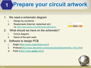
  • 3. Prepare your circuit artwork 1. We need a schematic diagram i. Design by ourselves ii. Readymade (Internet, datasheet etc) Eg. https://www.arduino.cc/en/Main/ArduinoBoardUno 2. What should we have on the schematic? i. Circuit diagram. ii. Name of the part used. 3. Software to design PCB i. Eagle (http://www.cadsoftusa.com/) ii. Proteus(http://www.labcenter.com/products/pcb/schematic_intro.cfm) iii. Pads (https://www.pads.com/) 1
  • 4. PCB Design Tutorial using Eagle Software Installing Download trial from http://www.cadsoftusa.com/download-eagle/ 1 Prepare your circuit artwork
  • 5. Create new project >File > New >Project A new project folder is made under the project. Set the name of the project folder by renaming. When the project is working, it isn't possible to change the name. In this case, select "Close Project" from the menu. When a project is closed, the green mark changes to the small gray mark. 1 Starting a New Project Prepare your circuit artwork
  • 6. The file to draw a schematic must be made after creating a project. Select "New" from the menu which is displayed by right clicking the project and select "Schematic". By above operation, the window to draw a schematic is displayed newly. In this condition, an actual file isn't made yet. 1 Create Schematic File Prepare your circuit artwork
  • 7. Select File menu and select "Save as...". The file is made with this operation. Write the name of the schematic. A file of .sch is saved by pushing the Save button. 1 Create Schematic File Prepare your circuit artwork
  • 8. 1 Create Board File Prepare your circuit artwork In the project, another important file must be createdcalled the board to draw the mask pattern for the printed board. The board file can be created after drawing a schematic. When adding a part to the schematic, a part is added to the board, too. So, when drawing a schematic, it is necessary to keep a board file always open condition. Click "Board" icon in the schematic window When a board isn't made yet, board creating is confirmed by following dialog.
  • 9. 1 Create Board File Prepare your circuit artwork Following board window is displayed. In this condition, an actual file isn't made yet. A board file is made by clicking "Save" icon in the board window. The file name is same as the schematic file. But, the extension is ".brd"
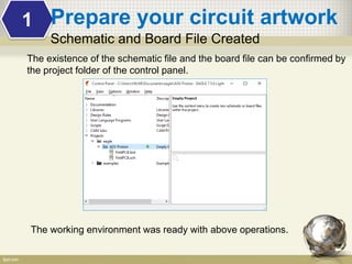
  • 10. 1 Schematic and Board File Created Prepare your circuit artwork The existence of the schematic file and the board file can be confirmed by the project folder of the control panel. The working environment was ready with above operations.
  • 11. 1 Selecting and Adding Parts Prepare your circuit artwork To make the mask pattern of the printed board, the schematic must be drawn. The part which is used with the schematic is chosen from the one which is registered on the library. Click the "ADD" button which is put on the left side in the schematic window. NOTE: this screen is displayed when the use status is active, marked by green bullet. Right click the Library folder and click Use All.
  • 12. 1 Selecting and Adding Parts Prepare your circuit artwork When pushing the OK button, a part is displayed on the schematic. Push the left button of the mouse in the position. Click one more to get another same part. To stop the addition function of the part, push an ESC key and "Cancel" button in the schematic window
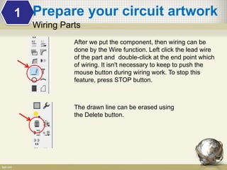
  • 13. 1 Wiring Parts Prepare your circuit artwork After we put the component, then wiring can be done by the Wire function. Left click the lead wire of the part and double-click at the end point which of wiring. It isn't necessary to keep to push the mouse button during wiring work. To stop this feature, press STOP button. The drawn line can be erased using the Delete button.
  • 14. 1 Exercise! Prepare your circuit artwork Draw this circuit now!.. A 5 volt voltage regulator circuit. After drawing a schematic, the mistake can be automatically detected by the ERC (Electrical Rule Check) button.
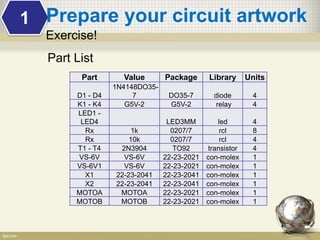
  • 15. 1 Exercise! Prepare your circuit artwork Part Value Package Library Units D1 - D4 1N4148DO35- 7 DO35-7 diode 4 K1 - K4 G5V-2 G5V-2 relay 4 LED1 - LED4 LED3MM led 4 Rx 1k 0207/7 rcl 8 Rx 10k 0207/7 rcl 4 T1 - T4 2N3904 TO92 transistor 4 VS-6V VS-6V 22-23-2021 con-molex 1 VS-6V1 VS-6V 22-23-2021 con-molex 1 X1 22-23-2041 22-23-2041 con-molex 1 X2 22-23-2041 22-23-2041 con-molex 1 MOTOA MOTOA 22-23-2021 con-molex 1 MOTOB MOTOB 22-23-2021 con-molex 1 Part List
  • 16. 1 Creating Board file Prepare your circuit artwork When the schematic drawing is ready, click Board button from schematic file. The yellow line among the parts is the line which shows a connection among the parts. But, these lines are not wiring for the printed board yet.
  • 17. 1 Parts arrangement on the board Prepare your circuit artwork The parts of the board are arranged out of the printed board. After pushing the Move button, move the parts inside the frame. We can also put text inside. The yellow line shows a connection among the parts. The part should be arranged for the yellow line to be simpler.
  • 18. 1 Autorouting on the board Prepare your circuit artwork Automatically wiring is done by the "Auto" button.