際際滷

際際滷Share a Scribd company logo
SCANNING TUNNELING
MICROSCOPY
SCANNING TUNNELING MICROSCOPY.pptx
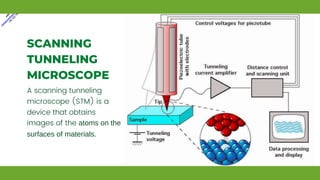
A scanning tunneling
microscope (STM) is a
device that obtains
images of the atoms on the
surfaces of materials.
SCANNING
TUNNELING
MICROSCOPE
SCANNING TUNNELING MICROSCOPY.pptx
ATOMIC SIZED PROBE
The STM is not an optical
microscope; instead, it works
by detecting electrical
forces with a probe that
tapers down to a point only
a single atom across
DETECTS ELECTRICAL
FORCES
STM DETECTS
IRREGULARITIES
ON THE SAMPLE
The electron shells, or clouds,
surrounding the atoms on
the surface produce
irregularities that are
detected by the probe and
mapped by a computer into
an image.
Quantum
tunneling
STM works on three key principles .
Piezo electric
effect
Feedback
current
KEY PRINCIPLES
 When the tip is brought very near to
the surface to be examined, a bias
voltage applied between the two allows
electrons to tunnel through the vacuum
separating them.
 The resulting tunneling current is a
function of the tip position, applied
voltage, and the local density of states
(LDOS) of the sample
QUANTUM TUNNELING
PRINCIPLE OF PIEZO ELEMENT.
THE APPLIED VOLTAGE MAKES
THE ELEMENT LONGER OR
SHORTER
5X10⁻⁷-5X10-12M,I.E.,A FRACTION OF ONE
MICROMETER TO ATOMIC
RESOLUTION
TRIPOD SCANNER
THE COMBINATION OF THREE PIEZO
ELEMENTS MAKES IT POSSIBLE TO
MOVE THE STM TIP IN THE X-, Y-, AND
Z-DIRECTIONS
TUBE SCANNER
IN MOST MODERN SCANNING
PROBE MICROSCOPES, ONE
USES A TUBE GEOMETRY.
 The tunneling current is amplified
by the current amplifier to
become a voltage.
 Which is compared with a reference
value
 The difference is then amplified
to drive the z peizo.
STM POSITIONING
.The phase of the amplifier
is chosen to provide
negative feedback:
If the tunneling current is
larger than the reference
value, then the voltage
applied to the z piezo tends
to withdraw the tip from the
sample surface, and vice
versa.
Doesnot work with insulators
Often needs to used under vacume
Able to obtain very high resolution images of conductors and semiconductors
Probe tips can be made out of thin wires
ADVANTAGES
DISADVANTAGES
THANKS
FOR YOUR TIME

More Related Content

SCANNING TUNNELING MICROSCOPY.pptx

  • 3. A scanning tunneling microscope (STM) is a device that obtains images of the atoms on the surfaces of materials. SCANNING TUNNELING MICROSCOPE
  • 5. ATOMIC SIZED PROBE The STM is not an optical microscope; instead, it works by detecting electrical forces with a probe that tapers down to a point only a single atom across DETECTS ELECTRICAL FORCES
  • 6. STM DETECTS IRREGULARITIES ON THE SAMPLE The electron shells, or clouds, surrounding the atoms on the surface produce irregularities that are detected by the probe and mapped by a computer into an image.
  • 7. Quantum tunneling STM works on three key principles . Piezo electric effect Feedback current KEY PRINCIPLES
  • 8. When the tip is brought very near to the surface to be examined, a bias voltage applied between the two allows electrons to tunnel through the vacuum separating them. The resulting tunneling current is a function of the tip position, applied voltage, and the local density of states (LDOS) of the sample QUANTUM TUNNELING
  • 9. PRINCIPLE OF PIEZO ELEMENT. THE APPLIED VOLTAGE MAKES THE ELEMENT LONGER OR SHORTER 5X10⁻⁷-5X10-12M,I.E.,A FRACTION OF ONE MICROMETER TO ATOMIC RESOLUTION TRIPOD SCANNER THE COMBINATION OF THREE PIEZO ELEMENTS MAKES IT POSSIBLE TO MOVE THE STM TIP IN THE X-, Y-, AND Z-DIRECTIONS TUBE SCANNER IN MOST MODERN SCANNING PROBE MICROSCOPES, ONE USES A TUBE GEOMETRY.
  • 10. The tunneling current is amplified by the current amplifier to become a voltage. Which is compared with a reference value The difference is then amplified to drive the z peizo.
  • 11. STM POSITIONING .The phase of the amplifier is chosen to provide negative feedback: If the tunneling current is larger than the reference value, then the voltage applied to the z piezo tends to withdraw the tip from the sample surface, and vice versa.
  • 12. Doesnot work with insulators Often needs to used under vacume Able to obtain very high resolution images of conductors and semiconductors Probe tips can be made out of thin wires ADVANTAGES DISADVANTAGES