狠狠撸

狠狠撸Share a Scribd company logo
Spintronics
     “A Spin to Remember”


Submitted To:-          Presented By:-
Er. Pieush Vyas         Abhishek Shringi
(Associate Professor)   08/33/106
(Unit In charge EC)     VIII Sem ECE
Outline

?   Spintronics basics
?   The giant magneto resistance
?   Applications of GMR
?   Spin devices
?   Injections & detection of spin
?   The MRAM
?   Recent trends
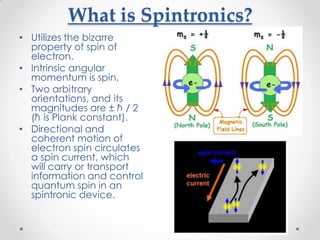
What is Spintronics?
? Utilizes the bizarre
  property of spin of
  electron.
? Intrinsic angular
  momentum is spin.
? Two arbitrary
  orientations, and its
  magnitudes are ± ? / 2
  (? is Plank constant).
? Directional and
  coherent motion of
  electron spin circulates
  a spin current, which
  will carry or transport
  information and control
  quantum spin in an
  spintronic device.
Why Spintronics?
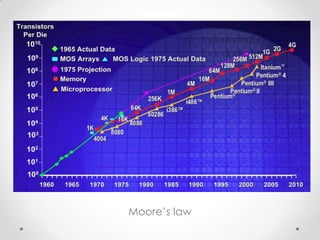
? Moore’s Law:
No. of Transistor doubles in every 18 months.

?Complexity:
Complex Chip Design & Power Loss.

? Motivation:
Spintronics-Information is carried not by electron
       charge but by it’s spin.
Moore’s law
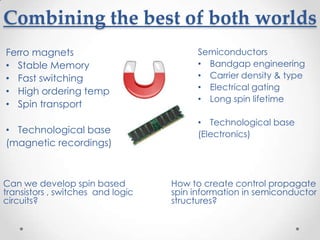
Combining the best of both worlds
Ferro magnets                            Semiconductors
? Stable Memory                          ? Bandgap engineering
? Fast switching                         ? Carrier density & type
? High ordering temp                     ? Electrical gating
                                         ? Long spin lifetime
? Spin transport
                                         ? Technological base
? Technological base                     (Electronics)
(magnetic recordings)


Can we develop spin based          How to create control propagate
transistors , switches and logic   spin information in semiconductor
circuits?                          structures?
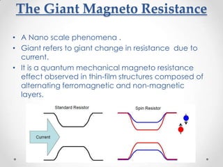
The Giant Magneto Resistance
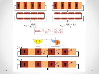
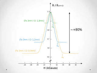
? A Nano scale phenomena .
? Giant refers to giant change in resistance due to
  current.
? It is a quantum mechanical magneto resistance
  effect observed in thin-film structures composed of
  alternating ferromagnetic and non-magnetic
  layers.
Spintronics ppt
Spintronics ppt
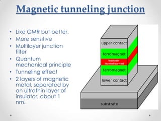
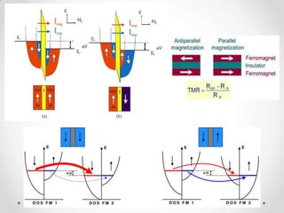
Magnetic tunneling junction

? Like GMR but better.
? More sensitive
? Multilayer junction
  filter
? Quantum
  mechanical principle
? Tunneling effect
? 2 layers of magnetic
  metal, separated by
  an ultrathin layer of
  insulator, about 1
  nm.
Spintronics ppt
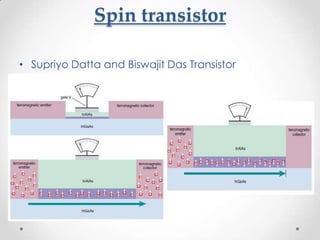
Spin transistor

? Supriyo Datta and Biswajit Das Transistor
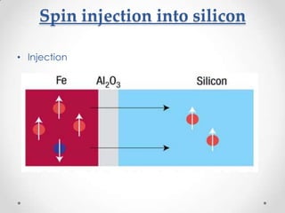
Spin injection into silicon

? Injection
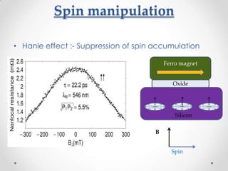
Spin manipulation

? Hanle effect :- Suppression of spin accumulation

                                          Ferro magnet


                                             Oxide


                                              Silicon

                                      B


                                            Spin
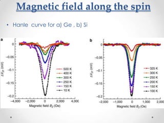
Magnetic field along the spin
? Hanle curve for a) Ge , b) Si
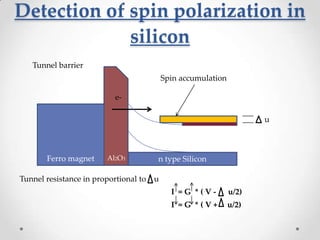
Detection of spin polarization in
             silicon
   Tunnel barrier
                                           Spin accumulation

                           e-

                                                                      u


       Ferro magnet     Al2O3          n type Silicon

Tunnel resistance in proportional to   u
                                             I =G *(V-         u/2)
                                             I =G *(V+         u/2)
MRAM
      Magneto resistive RAM
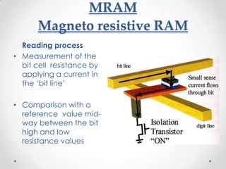
  Reading process
? Measurement of the
  bit cell resistance by
  applying a current in
  the ‘bit line’

? Comparison with a
  reference value mid-
  way between the bit
  high and low
  resistance values
MRAM
       Magneto resistive RAM
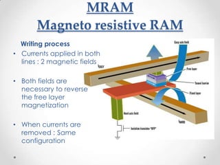
  Writing process
? Currents applied in both
  lines : 2 magnetic fields

? Both fields are
  necessary to reverse
  the free layer
  magnetization

? When currents are
  removed : Same
  configuration
MRAM
       Magneto resistive RAM
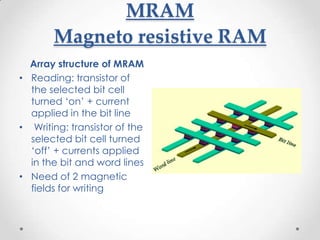
  Array structure of MRAM
? Reading: transistor of
  the selected bit cell
  turned ‘on’ + current
  applied in the bit line
? Writing: transistor of the
  selected bit cell turned
  ‘off’ + currents applied
  in the bit and word lines
? Need of 2 magnetic
  fields for writing
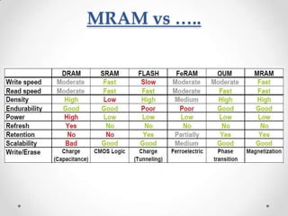
MRAM vs …..
MRAM
         Magneto resistive RAM


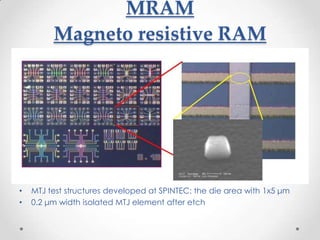
?   MTJ test structures developed at SPINTEC: the die area with 1x5 μm
?   0.2 μm width isolated MTJ element after etch
Advantages of Spintronics
? Low power consumption.

? Less heat dissipation.

? Spintronic memory is non-volatile.

? Takes up lesser space on chip, thus more compact.

? Spin manipulation is faster , so greater read & write speed.

? Spintronics does not require unique and specialized
  semiconductors.
  Common metals such as Fe, Al, Ag , etc. can be used.
Conclusion
? Spin property of electrons are yet to mastered.
? Researcher and scientist are taking keen interest.
? Universities and electronic industries collaborating .
? Span of last two decade major milestones.
? It holds vast opportunities for physics , material &
  device engineering & technology
? Last year PTB, Germany, have achieved a (2GBit/s)
  write cycle
? Potential of the field is colossal and
  continuous development is required.
Spintronics ppt
Spintronics ppt

More Related Content

Spintronics ppt

  • 1. Spintronics “A Spin to Remember” Submitted To:- Presented By:- Er. Pieush Vyas Abhishek Shringi (Associate Professor) 08/33/106 (Unit In charge EC) VIII Sem ECE
  • 2. Outline ? Spintronics basics ? The giant magneto resistance ? Applications of GMR ? Spin devices ? Injections & detection of spin ? The MRAM ? Recent trends
  • 3. What is Spintronics? ? Utilizes the bizarre property of spin of electron. ? Intrinsic angular momentum is spin. ? Two arbitrary orientations, and its magnitudes are ± ? / 2 (? is Plank constant). ? Directional and coherent motion of electron spin circulates a spin current, which will carry or transport information and control quantum spin in an spintronic device.
  • 4. Why Spintronics? ? Moore’s Law: No. of Transistor doubles in every 18 months. ?Complexity: Complex Chip Design & Power Loss. ? Motivation: Spintronics-Information is carried not by electron charge but by it’s spin.
  • 6. Combining the best of both worlds Ferro magnets Semiconductors ? Stable Memory ? Bandgap engineering ? Fast switching ? Carrier density & type ? High ordering temp ? Electrical gating ? Long spin lifetime ? Spin transport ? Technological base ? Technological base (Electronics) (magnetic recordings) Can we develop spin based How to create control propagate transistors , switches and logic spin information in semiconductor circuits? structures?
  • 7. The Giant Magneto Resistance ? A Nano scale phenomena . ? Giant refers to giant change in resistance due to current. ? It is a quantum mechanical magneto resistance effect observed in thin-film structures composed of alternating ferromagnetic and non-magnetic layers.
  • 10. Magnetic tunneling junction ? Like GMR but better. ? More sensitive ? Multilayer junction filter ? Quantum mechanical principle ? Tunneling effect ? 2 layers of magnetic metal, separated by an ultrathin layer of insulator, about 1 nm.
  • 12. Spin transistor ? Supriyo Datta and Biswajit Das Transistor
  • 13. Spin injection into silicon ? Injection
  • 14. Spin manipulation ? Hanle effect :- Suppression of spin accumulation Ferro magnet Oxide Silicon B Spin
  • 15. Magnetic field along the spin ? Hanle curve for a) Ge , b) Si
  • 16. Detection of spin polarization in silicon Tunnel barrier Spin accumulation e- u Ferro magnet Al2O3 n type Silicon Tunnel resistance in proportional to u I =G *(V- u/2) I =G *(V+ u/2)
  • 17. MRAM Magneto resistive RAM Reading process ? Measurement of the bit cell resistance by applying a current in the ‘bit line’ ? Comparison with a reference value mid- way between the bit high and low resistance values
  • 18. MRAM Magneto resistive RAM Writing process ? Currents applied in both lines : 2 magnetic fields ? Both fields are necessary to reverse the free layer magnetization ? When currents are removed : Same configuration
  • 19. MRAM Magneto resistive RAM Array structure of MRAM ? Reading: transistor of the selected bit cell turned ‘on’ + current applied in the bit line ? Writing: transistor of the selected bit cell turned ‘off’ + currents applied in the bit and word lines ? Need of 2 magnetic fields for writing
  • 21. MRAM Magneto resistive RAM ? MTJ test structures developed at SPINTEC: the die area with 1x5 μm ? 0.2 μm width isolated MTJ element after etch
  • 22. Advantages of Spintronics ? Low power consumption. ? Less heat dissipation. ? Spintronic memory is non-volatile. ? Takes up lesser space on chip, thus more compact. ? Spin manipulation is faster , so greater read & write speed. ? Spintronics does not require unique and specialized semiconductors. Common metals such as Fe, Al, Ag , etc. can be used.
  • 23. Conclusion ? Spin property of electrons are yet to mastered. ? Researcher and scientist are taking keen interest. ? Universities and electronic industries collaborating . ? Span of last two decade major milestones. ? It holds vast opportunities for physics , material & device engineering & technology ? Last year PTB, Germany, have achieved a (2GBit/s) write cycle ? Potential of the field is colossal and continuous development is required.