Spintronics
- 1. University College Of Engineering, Rajasthan Technical University, Kota.Presentation OnSpintronics Technology Submitted To: Presented By :Dr R S MeenaShailendra Kumar Singh MrPankajShukla C.R. No : 07/126 Final B. Tech. (ECE)
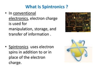
- 2. What Is Spintronics ?In conventional electronics, electron charge is used for manipulation, storage, and transfer of information .Spintronics uses electron spins in addition to or in place of the electron charge.
- 3. Why We Need Spintronics !Failure of MooreĄŊs Law : MooreĄŊs Law states that the number of transistors on a silicon chip will roughly double every eighteen months. But now the transistors & other components have reached nanoscale dimensions and further reducing the size would lead to: 1. Scorching heat making making the circuit inoperable. 2. Also Quantum effects come into play at nanoscale dimensions.So the size of transistors & other components cannot be reduced further.
- 4. Basic Principle In Spintronics , information is carried by orientation of spin rather than charge. Spin can assume one of the two states relative to the magnetic field, called spin up or spin down. These states, spin up or spin down, can be used to represent ĄŪ1ĄŊ and ĄŪ0ĄŊ in binary logic. In certain spintronic materials, spin orientation can be used as spintronic memory as these orientation do not change when system is switched off.
- 5. Advantage Spintronics Low power consumption.
- 7. Spintronic memory is non-volatile.
- 8. Takes up lesser space on chip, thus more compact.
- 9. Spin manipulation is faster , so greater read & write speed.
- 10. Spintronics does not require unique and specialized semiconductors. Common metals such as Fe, Al, Ag , etc. can beused.
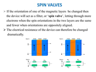
- 11. GaintMagnetoresistance (GMR)The basic GMR device consists of a layer of non -magnetic metal between two two magnetic layers. A current consisting of spin-up and spin-down electrons is passed through the layers. Those oriented in the same direction as the electron spins in a magnetic layer pass through quite easily while those oriented in the opposite direction are scattered.
- 12. SPIN VALVESIf the orientation of one of the magnetic layers be changed then the device will act as a filter, or ĄŪspin valveĄŊ, letting through more electrons when the spin orientations in the two layers are the same and fewer when orientations are oppositely aligned. The electrical resistance of the device can therefore be changed dramatically.
- 13. Tunnel Magnetoresistance Magnetic tunnel junction has two magnetic layers separated by an insulating metal-oxide layer. Is similar to a GMR spin valve except that a very thin insulator layer is sandwitched between magnetic layers instead of metal layer . The difference in resistance between the spin-aligned and nonaligned cases is much greater than for GMR device ĻC infact 1000 times higher than the standard spin valve.
- 14. Magnetoresistive Random Access Memory (MRAM) MRAM uses magnetic storage elements.
- 15. The elements are mostly tunnel junctions formed from two ferromagnetic plates, each of which can hold a magnetic field, separated by a thin insulating layer.
- 16. SRAM VS DRAM VS MRAMSRAMDRAMMRAMAdvantage Fast read & write speed. Low power
- 17. High density
- 18. Fast read &write speed.Fast read &write speed. Low power
- 19. High density
- 20. Non VolatileDisadvantage Volatile
- 21. Low density
- 22. Volatile
- 23. High power
- 24. None ??Comparison with DRAM & SRAM In DRAM & SRAM, a bit is represented as charge stored in capacitor. In MRAM, data is stored as magnetic alignment of electrons in a ferromagnetic material. Spin up represents ĄŪ0ĄŊ and spin down represents ĄŪ1ĄŊ. MRAM promises:
- 25. Density of DRAM
- 26. Speed of SRAM
- 27. Non-volatility like flash memory.
- 28. ThatĄŊs why its called universal memory.256 K MRAM
- 29. Journey of MRAMProblems encountered: 1. The density of bits was low. 2. Cost of chips was high. Improved designs to overcome these problems would work only at liquid nitrogen temperature. An important breakthrough was made in the year 2009.
- 30. Scientists at the North Carolina State University discovered a semiconductor material ĄŪ Galium manganese nitrideĄŊ that can store & retain spin orientation at room temperature. And research is still going onĄ Thanks for your attentionĄ!!!Any Queries ??
Editor's Notes
- #3: Spin does not replace charge current just provide extra controlUsing suitable materials, many different Ą°bitĄą states can be interpreted
