SRAM DRAM
âĒDownload as PPTX, PDFâĒ
9 likesâĒ7,586 views

This document is a presentation on RAM that was presented by Tipu Sultan and Md Shakhawat Hossain Sujon to Tafisr Ahmed Khan. It summarizes the key differences between SRAM and DRAM. SRAM does not require refresh cycles but is more expensive and slower than DRAM. A typical SRAM cell uses 6 transistors arranged in two cross-coupled inverters, while a DRAM cell uses one transistor and one capacitor. DRAM must perform periodic refresh cycles to maintain its data due to capacitor leakage, whereas SRAM maintains its data statically without refresh.


SRAM DRAM
- 2. A Presentation on Ram Presented by ïĩ Tipu Sultan ïĩ Roll:04 ïĩ Batch: 17th ïĩ Md Shakhawat Hossain Sujon ïĩ Roll: 02 ïĩ Batch: 17th Presented to ïĩ TAFSIR AHMED KHAN ïĩ LECTURER ïĩ DEPARTMENT OF EETE ïĩ DHAKA INTERNATIONAL UNIVERSITY 4/5/2017 2
- 3. Random Access Memory (RAM) Static RAM Dynamic RAM 4/5/2017 3
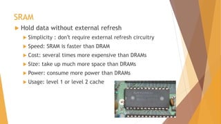
- 4. SRAM ïĩ Hold data without external refresh ïĩ Simplicity : donât require external refresh circuitry ïĩ Speed: SRAM is faster than DRAM ïĩ Cost: several times more expensive than DRAMs ïĩ Size: take up much more space than DRAMs ïĩ Power: consume more power than DRAMs ïĩ Usage: level 1 or level 2 cache 4/5/2017 4
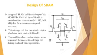
- 5. Design Of SRAM ï A typical SRAM cell is made up of six MOSFETs. Each bit in an SRAM is stored on four transistors (M1, M2, M3, M4) that form two cross-coupled inverters. ï This storage cell has two stable states which are used to denote 0 and 1. ï Two additional access transistors serve to control the access to a storage cell during read and write operations. 4/5/2017 5
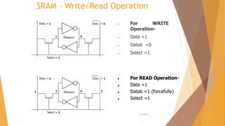
- 6. SRAM â Write/Read Operation ïŽ For WRITE Operation- ïŽ Data =1 ïŽ Datab =0 ïŽ Select =1 ïŽ For READ Operation- ïŽ Data =1 ïŽ Datab =1 (forcefully) ïŽ Select =1 4/5/2017 6
- 7. Reading operation ï Assume that the content of memory is 1 stored at Q. The read cycle is started by precharging both the bit lines to a logic 1, ï The word line WL, enabling M5 AND M6 . ï The second step occurs when the value stored in Q & Qâ are transferred to the bit line by leaving BL at its precharged value and discharging BLâ through M1 and M5 to a logical 0 ï On the BL side, the transistors M4 and M6 pull the bit line toward VDD, a logical 1 (M4 as it is turned on because Qâ is logically set to 0). ï Bit lines reach a sense amplifier, which will sense which line has higher voltage and thus will tell whether there was 1 stored or 0. The higher the sensitivity of sense amplifier, the faster the speed of read operation is. 4/5/2017 7
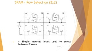
- 8. SRAM â Row Selection (2x2) ïŽ - Simple inverted input used to select between 2 rows 4/5/2017 8
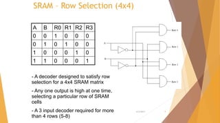
- 9. SRAM â Row Selection (4x4) A B R0 R1 R2 R3 0 0 1 0 0 0 0 1 0 1 0 0 1 0 0 0 1 0 1 1 0 0 0 1 - A decoder designed to satisfy row selection for a 4x4 SRAM matrix - Any one output is high at one time, selecting a particular row of SRAM cells - A 3 input decoder required for more than 4 rows (5-8) 4/5/2017 9
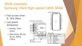
- 11. SRAM example: Samsung 1Mx4 High-speed CMOS SRAM ïĩ Fast access time: 8, 10ns (Max) ïĩ Low power dissipation ïĩ Stanby: 5mA (max) ïĩ Operating: 80 mA (8 ns), 65mA (10ns) 4/5/2017 11
- 13. DRAM Dynamic Random Access Memory ï Basic storage device is not a flip flop but a MOS and a capacitor ï Charge determine the stored bit (0,1) ï Data stored as a charge not remain infinitely due to leakage current, therefore periodic refresh cycle is required to maintain stored data. 4/5/2017 13
- 14. OPERATION VDD O/P CT1 T3 I/P A ï When A= 1 T1 will be ON then capacitor charges to I/P value during interval A=1 ïWhen T1 is OFF the invertor will remember the sample data because of stored charge on capacitor. ïCharge on capacitor eventually leak OFF. Because of leakage through insulation which supports the gate on T2. ï To larger extent it is due to leakage through reverse biased junction formed b/w sub. And drain of T1. 4/5/2017 14
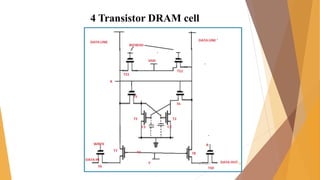
- 15. 4 Transistor DRAM cell 4/5/2017 15
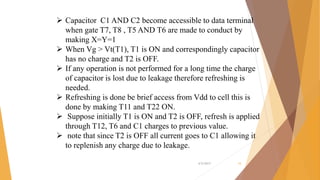
- 16. ï Capacitor C1 AND C2 become accessible to data terminal when gate T7, T8 , T5 AND T6 are made to conduct by making X=Y=1 ï When Vg > Vt(T1), T1 is ON and correspondingly capacitor has no charge and T2 is OFF. ï If any operation is not performed for a long time the charge of capacitor is lost due to leakage therefore refreshing is needed. ï Refreshing is done be brief access from Vdd to cell this is done by making T11 and T22 ON. ï Suppose initially T1 is ON and T2 is OFF, refresh is applied through T12, T6 and C1 charges to previous value. ï note that since T2 is OFF all current goes to C1 allowing it to replenish any charge due to leakage. 4/5/2017 16
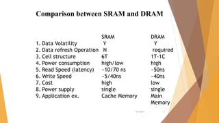
- 17. SRAM DRAM 1. Data Volatility Y Y 2. Data refresh Operation N required 3. Cell structure 6T 1T-1C 4. Power consumption high/low high 5. Read Speed (latency) ~10/70 ns ~50ns 6. Write Speed ~5/40ns ~40ns 7. Cost high low 8. Power supply single single 9. Application ex. Cache Memory Main Memory Comparison between SRAM and DRAM 4/5/2017 17