System Hierarchy in Printed Electronics
- 1. System Hierarchy in Printed Electronics Dr. Andreas Schaller ASC Andreas Schaller Technology Consulting info@andreas-schaller.de Dr. Andreas Schaller System Hierarchy in Printed Electronics 1
- 2. Overview System Hierarchy in Printed Electronics2 1. Introduction 2. IEEE Electronics System Hierarchy 3. Costs 4. Environment 5. Summary S
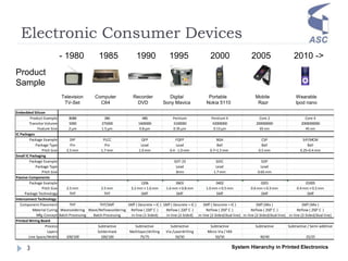
- 3. Electronic Consumer Devices System Hierarchy in Printed Electronics3 1985 1990 1995 2000 2005 2010 ->- 1980 Television TV-Set Computer C64 Recorder DVD Digital Sony Mavica Portable Nokia 5110 Mobile Razr Wearable Ipod nano Embedded Silicon Product Example 8088 386 486 Pentium Pentium 4 Core 2 Core 4 Transitor Volume 5000 275000 1600000 3100000 42000000 200000000 2000000000 Feature Size 2 ┬Ąm 1.5 ┬Ąm 0.8 ┬Ąm 0.35 ┬Ąm 0.13 ┬Ąm 65 nm 45 nm IC Packages Package Example DIP PLCC QFP FQFP BGA CSP SiP/MCM Package Type Pin Pin Lead Lead Ball Ball Ball Pitch Size 2.5 mm 1.7 mm 1.0 mm 0.4 - 1.0 mm 0.7ŌĆō1.5 mm 0.5 mm 0.25ŌĆō0.4 mm Small IC Packaging Package Example SOT-23 SOIC SOP Package Type Lead Lead Lead Pitch Size 3mm 1.7 mm 0.65 mm Passive Components Package Example 1206 0603 0402 0201 01005 Pitch Size 2.5 mm 2.5 mm 3.2 mm ├Ś 1.6 mm 1.6 mm ├Ś 0.8 mm 1.0 mm ├Ś 0.5 mm 0.6 mm ├Ś 0.3 mm 0.4 mm ├Ś 0.2 mm Package Technology THT THT SMT SMT SMT SMT SMT Interconnect Technology Component Placement THT THT/SMT SMT ( Descrete + IC ) SMT ( Descrete + IC ) SMT ( Descrete + IC ) SMT (Mix ) SMT (Mix ) Material Curing Wavesoldering Wave/Reflowsoldering Reflow ( 220┬░ C ) Reflow ( 220┬░ C ) Reflow ( 250┬░ C ) Reflow ( 250┬░ C ) Reflow ( 250┬░ C ) Mfg-Concept Batch Processing Batch Processing in-line (1-Sided) in-line (2-Sided) in-line (2-Sided/dual line) in-line (2-Sided/dual line) in-line (2-Sided/dual line) Printed Wiring Board Process Subtractive Subtractive Subtractive Subtractive Subtractive Subtractive / Semi-additive Layers Soldermask Multilayer/drilling Via /Laserdrilling Micro-Via / HDI Line Space/Width 100/100 100/100 75/75 50/50 50/50 40/40 25/25 Product Sample
- 4. Future ICT Markets ŌĆØInternet of ThingsŌĆØ System Hierarchy in Printed Electronics4 Green Cars Factories of the Future Energy-efficient Buildings Future Internet ŌĆó Microelectronics ŌĆó Ubiquitous positioning ŌĆó Wirelessly communicating smart systems ŌĆó Non-silicon based components ŌĆó Energy harvesting technologies ŌĆó Privacy- and security-by-design Surface Mount Technology Printed Technology Embedded Intelligence Integrated Smart Systems
- 5. Electronic Consumer Devices (Future Internet ) System Hierarchy in Printed Electronics5 GPS Library Social Networks Location AR Payment Coupons Loyalty TV/Cinema Flight Ticketing Product Info Wellness Ticketing Gaming Sport B2C OLED Smart Packaging Diagnosis Large Area Sensors Future Internet
- 6. Integrated Smart Systems Main devices and applications System Hierarchy in Printed Electronics6
- 7. IEEE Electronics System Hierarchy System Hierarchy in Printed Electronics7
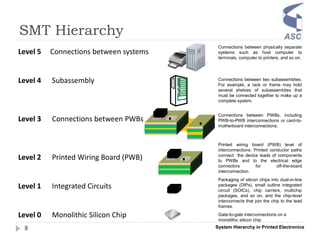
- 8. SMT Hierarchy System Hierarchy in Printed Electronics8 Connections between physically separate systems such as host computer to terminals, computer to printers, and so on. Level 5 Connections between systems Level 4 Subassembly Level 3 Connections between PWBs Level 2 Printed Wiring Board (PWB) Level 1 Integrated Circuits Level 0 Monolithic Silicon Chip Gate-to-gate interconnections on a monolithic silicon chip Connections between two subassemblies. For example, a rack or frame may hold several shelves of subassemblies that must be connected together to make up a complete system. Connections between PWBs, including PWB-to-PWB interconnections or card-to- motherboard interconnections. Printed wiring board (PWB) level of interconnections. Printed conductor paths connect the device leads of components to PWBs and to the electrical edge connectors for off-the-board interconnection. Packaging of silicon chips into dual-in-line packages (DIPs), small outline integrated circuit (SOICs), chip carriers, multichip packages, and so on, and the chip-level interconnects that join the chip to the lead frames.
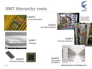
- 9. SMT Hierarchy roots System Hierarchy in Printed Electronics9 Level 0 Level 1 Level 2 Level 3 Level 4 Level 5 on-chip interconnects Packaging PCB level (assembly) Inter PCB connections Inter rack connections Inter systems connections Source : Various maris techcon, SSI, Como 2010
- 10. Printed Electronics (PET) System Hierarchy in Printed Electronics10 Source : Acreo
- 11. PET Hierarchy System Hierarchy in Printed Electronics11 Level 5 Connections between systems Ambient Intelligence Level 4 Subassembly System Integration Level 3 Connections between PWBs Smart System Level 2 Printed Wiring Board (PWB) System-in-Foil Level 1 Integrated Circuits Functional Layers Level 0 Monolithic Silicon Chip Printable Ink Silver Ink Printed Antenna RFID Label Battery Assisted Label Smart Package RFID System SMT PET Example
- 12. PET Applications System Hierarchy in Printed Electronics12 OE-A Roadmap Products
- 13. Costs System Hierarchy in Printed Electronics13
- 14. Integrated Smart Systems Costs System Hierarchy in Printed Electronics14 Ink (Organic and/or Inorganic) Foils and/or Paper Inkjet / Gravure / Screen Printing Assembly (Lamination) Lamination Labeling (none if integrated) Battery and/or IC Antenna and/or Sensor Connectingwire / wireless Tagged Object ( included in BOM)
- 15. Optimized Costs System Hierarchy in Printed Electronics15 RFID RFID Printing Foils Added Value ?
- 16. System on Foils System Hierarchy in Printed Electronics16 Source: iNEMI Roadmap on INTERCONNECTION SUBSTRATES - ORGANIC Antenna RF Logic Sensor 4 layers could be the limit before the alignment costs become the bottleneck Assumption: >100 ╬╝m feature size Ratio of differences in cost per layer
- 17. Integrated Smart Systems EU Project Demonstrators System Hierarchy in Printed Electronics17 0% 10% 20% 30% 40% 50% 60% 70% 80% 90% 100% 3Plast Level 3 - CC Level 3 - BOM Level 2 - CC Level 1 - CC Level 1 - BOM Level 0 - BOM 0% 10% 20% 30% 40% 50% 60% 70% 80% 90% 100% PriMeBits Level 3 - CC Level 3 - BOM Level 2 - CC Level 1 - CC Level 1 - BOM Level 0 - BOM Intelligent Surfaces Smart Card Memory / Battery / Conductor Inorganic R2R Gravure + Screen Display / Pyro Sensor / ECT Organic / Hybrid R2R (Inkjetting+Screen) Not Included Cost%Cost%
- 18. Large Area Sensors Integrated Pyro/Piezoelectric Sensors Integrated organic physical sensor ŌĆó Capacitive sensor part is based on ferroelectric polymer ŌĆó Sensor response to ╬öT, ╬öp controls the transistorŌĆ×s gate ŌĆó Transistor transforms high-impedance sensor signal to low-impedance output signal ŌĆó Monolithically integrated on flexible substrate Sensor Transistor System Hierarchy in Printed Electronics18
- 19. p ~ 40 ┬ĄC/m2K d33 = 24 pC /N Sensor and Transistors System Hierarchy in Printed Electronics19 VG VDS VG VDS Sensor Transistors
- 20. Integrated Sensor Manufacturing Sensor Function Material Foil PET Bottom Electrode PEDOT:PSS Piezo / Pyro PVDF-TrFE Top Electrode Carbon Transistor Function Material Process Foil PET Screen Contacts Carbon Channel PEDOT:PSS Inkjet Lacquer Su2 Electrolyte Electrolyte System Hierarchy in Printed Electronics20
- 21. Human-Machine Interface All-printed sensor with ACREO display ŌĆó Control with/without touch ŌĆó Minimized number of materials ŌĆó Large Areas Electronics ŌĆó Very robust System Hierarchy in Printed Electronics21 http://cid-2e87bf9055410c4c.photos.live.com/self.aspx/ASC-Andreas%20Schaller%20Technology%20Consulting/3Plast.wmv
- 22. HMI Applications SensorFunctionality Sort Select PointArray PointArray Several Suppliers 3Plast Demonstrator Several Suppliers Source : GestIC Source : gesture-cube Laser Source : Microsoft Source : Apple Sensor TypeDo not touch Source : Motorola Can not touch SensorFunctionality Sort Select Sensor Type System Hierarchy in Printed Electronics22
- 23. 0% 10% 20% 30% 40% 50% 60% 70% 80% 90% 100% Integrated Smart Systems Costs Analysis ( Examples ) System Hierarchy in Printed Electronics23 0% 10% 20% 30% 40% 50% 60% 70% 80% 90% 100% Level 3 - CC Level 3 - BOM Level 2 - CC Level 1 - CC Level 1 - BOM Level 0 - BOM 0% 10% 20% 30% 40% 50% 60% 70% 80% 90% 100% Level 3 - CC Level 3 - BOM Level 2 - CC Level 1 - CC Level 1 - BOM Level 0 - BOM 0% 10% 20% 30% 40% 50% 60% 70% 80% 90% 100% Smart Card Intelligent Surfaces OLED Shelf OLED Display Cost%Cost% Cost%Cost%
- 24. Environment System Hierarchy in Printed Electronics24
- 25. Sustainability System Hierarchy in Printed Electronics25 Environmental Impact EoL / Recycling Compliance Energy / CO2 Footprint Social Impact Economic Impact See Cost ║▌║▌▀Ż See Application ║▌║▌▀Ż Material (Level 0) : ROHS / REACH Energy (Level 5) : EUP Disassembly (Level 3) : WEEE Smart Card (Level 1) : Drying/Sintering ( depends on application )
- 26. Social Impact Smart Packaging drives Pharmacy Services System Hierarchy in Printed Electronics26 ┬® Stora Enso ┬® Stora Enso ┬® Stora Enso Pharmacy Logistics Personal Care Medical Compliance http://www.rfidjournal.com/article/view/7848 http://81.209.16.38/Link.aspx?id=1034686 http://www.rfidjournal.com/article/view/7785 - Digital content driven services in pharmacy needs new smart packaging solutions - Smoother integration of electronics in packaging is required Data Logging Event Detection Human Machine Interface
- 27. Medical Compliance Low Cost Printed Memory System Hierarchy in Printed Electronics27 14-bit inkjetted WORM bank Uwrite= 10 V and Rs= 330 ╬®. ŌĆóresistive memory: electrically induced sintering high-resistance->low-resistance) ŌĆókey point : electrically post-fabrication programmable
- 28. Economic Impact Improved Memory System Hierarchy in Printed Electronics28 Demonstration roll-to-roll run ŌĆó direct gravure ŌĆó produced length > 150m (> 10 000 memory banks) ŌĆó roll-to-roll die-cut ŌĆó encapsulation: manual hot lamination ROKO pilot line┬® VTT ┬® VTT ┬® VTT ┬® EPFL ┬®Nicanti Fully Optimized Memory Costs ~ 1 cent
- 29. Economic Impact Medical Compliance Card System Hierarchy in Printed Electronics29
- 30. Environmental Impact Recycling System Hierarchy in Printed Electronics30 Running electronics thru paper recycling Yield ~ 95 % Yield ~ 50 % Yield ~ 98 %
- 31. Technology Comparison System Hierarchy in Printed Electronics31 SMT PET $$$ (BOM/CC) 4-5 Ōé¼ Target 1-2 Ōé¼ CO2 (Footprint) ~ 2,25 kg ~ 1,18 kg WEEE (Recycling Rate) ~ 67 % ~ 73 % ROHS Passed Passed
- 32. Technology Comparison System Hierarchy in Printed Electronics32 $$$CO2 Assumptions : - Production environment not included - Battery MFG not included, only BOM - Recycling not included
- 33. CO2 Footprint System Hierarchy in Printed Electronics33 1. Use Phase As there is no long use phase for ŌĆ×disposableŌĆ£ smart packaging the CO2 impact depends on the manufacturing phase. 2. Manufacturing phase The drying / sintering processes are the main driver for level 1. This needs to be optimized ! 3. Printed Electronics Moving into a clean room environment for production would significantly decrease the CO2 benefits of PET vs. SMT 4. Organic Electronics What would have changed if we had used organic material ?
- 34. Environmental Impact Printed Electronics System Hierarchy in Printed Electronics34 Improvement in % PET vs. SMT ROHS Compliance Economic Mfg Costs Lifecycle CO2-Footprint WEEE Recycling Rate Summary SMT/PET fully passed 60% 48% 10% Technology Energy for production (MJ.Wp-1) CO2 footprint (gr.CO2-eq.Wp-1) Energy payback time (years) mc-Si 24,9 1293 1,95 CdTe 9,5 542 0,75 CIS 34,6 2231 2,71 OPV 2,4 132 0,19 Source : A. L. Roes et al, Progress in Photovoltaics 17, 372 (2009) Source : Konarka Source : Sumitomo Chemical Source : PriMeBits OPV Smart Packaging Source : Sony Source : LG OLED
- 35. Summary System Hierarchy in Printed Electronics35 Smart Objects are driven by LEVEL 5 (Content driven) Connectivity enables an object to become ŌĆØsmartŌĆØ Flexible Electronics is driven by LEVEL 4 Customer Benefits is flexible-to-install vs. flexible-to-use Integrated Smart Systems are driven by LEVEL 3 Application driven system integration Large Area Electronics is driven by LEVEL 2 Macro electronics for functional area maximization (vs. microminiaturization) Printed Electronics is driven by LEVEL 1 Low cost and environmental preferred manufacturing Organic(Inorganic) Electronics is driven by LEVEL 0 Multi-functional materials for electronic and sensing functions
- 36. Roadmapping System Hierarchy in Printed Electronics36 2011 Roadmap on Large Area Flexible Electronics Published 01/2011
- 37. PE has to evolve from a low cost to an enabling technology System Hierarchy in Printed Electronics37 Source : Thin Film Source : PolyIC Source : Polymer Vision / Wistron Source : Stora Enso Source : Sensible Solutions Source : Prelonic Source : NTERA FLEXIBILITY ! TRANSPARENCY ! CONNECTIVITY !
- 38. Questions ? System Hierarchy in Printed Electronics38 Andreas Schaller Technology Consulting Unternehmergesellschaft (haftungsbeschr├żnkt) Dr. Andreas Schaller Email : andreas@andreas-schaller.de Andreas Schaller Technology Consulting Unternehmergesellschaft (haftungsbeschr├żnkt) Office : Schulstr. 11, 95676 Wiesau Management : Dr. Andreas Schaller District Court : AG Weiden, HRB 3499

