The look up table (LUT)
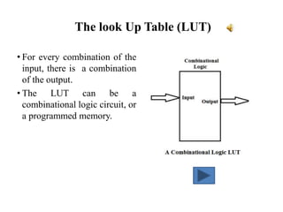
- 1. The look Up Table (LUT) • For every combination of the input, there is a combination of the output. • The LUT can be a combinational logic circuit, or a programmed memory.
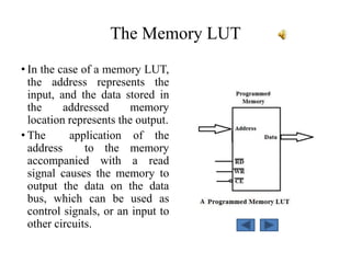
- 2. The Memory LUT • In the case of a memory LUT, the address represents the input, and the data stored in the addressed memory location represents the output. • The application of the address to the memory accompanied with a read signal causes the memory to output the data on the data bus, which can be used as control signals, or an input to other circuits.
- 3. Producing a repetitive waveform • The required form of the signals [S3-S0] are stored in five memory locations ( location 0 to location 4) as [D3-D0]. • The sequence of these signal forms is extracted from successive memory location with each clock cycle.
- 4. A programmed Memory LUT Circuit •The circuit is composed of an EPROM, a 3-bit counter, a NAND gate, and two switches. •The push button clears the counter. When the button is released, the output of the NAND gate (logic 1) enables the count and disables the Clear, and the count (C2-C0) is increased with the rising edge of each clock cycle, i.e., the next memory location is addressed.
- 5. The EPROM LUT; Continue * So, with each new clock cycle, a new memory location is addressed and its contents are output on the data bus to be used as control signals [S3-S0]. • When the count reaches 5Hex (101 binary), the output of the NAND gate becomes logic 0. This clears the counter to start again. • So the form is repeated every five clock cycles.


![Producing a repetitive waveform
• The required form of the
signals [S3-S0] are stored in
five memory locations (
location 0 to location 4) as
[D3-D0].
• The sequence of these signal
forms is extracted from
successive memory location
with each clock cycle.](https://image.slidesharecdn.com/thelookuptablelut-151024190136-lva1-app6891/85/The-look-up-table-LUT-3-320.jpg)

![The EPROM LUT; Continue
* So, with each new clock
cycle, a new memory
location is addressed and its
contents are output on the
data bus to be used as
control signals [S3-S0].
• When the count reaches
5Hex (101 binary), the
output of the NAND gate
becomes logic 0. This clears
the counter to start again.
• So the form is repeated
every five clock cycles.](https://image.slidesharecdn.com/thelookuptablelut-151024190136-lva1-app6891/85/The-look-up-table-LUT-5-320.jpg)