Tsfpga
âĒDownload as PPTX, PDFâĒ
2 likesâĒ349 views

This document discusses the Matrix, TSFPGA, and DPGA architectures. Matrix is based on an array of identical primitive elements with a configurable interconnect network. It operates in a pipelined fashion. TSFPGA moves the value registers to the inputs of computational elements, allowing values to move between producer and consumer with minimum transit time independent of when the consumer will use the data. It uses input registers and broadcasts the current timestep so inputs can load values when their programmed load time matches. The basic building block of TSFPGA is the subarray tile containing LUTs and a central crossbar for switching.


Tsfpga
- 1. MATRIX ,TSFGA & DPGA By Bhavana Sawant & Pranoti Bachhav
- 2. Matrix concepts ï Matrix is designed to maintain flexibility in Instruction control. ï Matrix is based on a uniform array of primitive elements and interconnect which can serve instruction control and data functions. ï The key to providing this flexibility is a multilevel configuration scheme which allows device to control the way it deliver configuration information.
- 3. Matrix architecture ï Matrix microarchitecture is based around an array of identical 8 bit primitive datapath elements overlayed with a confiqurable network
- 5. Basic functional unit 1) 256x8 memory = function as a Single 256 byte ,dual ported and 128 X 8 bit In register file mode the memoy supports two reads and one write operation on each cycle. 2) 8- bit ALU=set of arithmatic and logic functions 3) Control logic=Composed of 1) Local pattern matcher for generating local control from the ALU output 2)a reduction network for generating local control 3) a 20- input 8-output NOR block which can serve as half of PLA
- 6. MATRIX operation âĒ Matrix operation is pipelined at the BFU level with pipeline register at each BFU input port. âĒ Pipeline stage includes: I. Memory read II. ALU operation III. Memory write and local interconnect traversal= two operations proceed in parallel BFU role -I store -Data memory -ALU function
- 7. Matrix network âĒ Collection of a 8 bit busses âĒ Dynamically switch network connections 1.Nearest neighbor Connection= connection between BFU and two grid squares 2.Length four bypass connection=each BFU support level two connections - Which allows corner turns ,local fanout, medium distance interconnect, data shifting and retiming 3.Global Lines-every row and column supports four interconnects lines which span the entire row or column.
- 8. MATRIX example âĒ Finite Impulse Response filter
- 9. Dynamically Programmable Gate Arrays with Input Registers âĒ We must hold the value on the output and tie up switches and wires between the producer and the consumer until such time as the final consumer has used the value. âĒ Switches and wires are forced to sit idle holding values for much longer than the time. The alternative is to move the value registers to the inputs of the computational elements. âĒ These input registers allow us to store values which need to traverse LUT evaluation levels in memories rather than having them consume active resources during the period of time which they are being retimed
- 10. Input Registers Having four flip-flops on the input of each 4-LUT rather than one flip-flop on the output. This modification allows us to move the data from the producer to consumer in the minimum transit time -- a time independent of when the consumer will actually use the data. Conceptually, the key idea here is that signal transport and retiming are two different functions: âĒ Spatial Transport -- moves data in space -- route data from source to destination âĒ Temporal Transport (Retiming) -- moves data in time -- make data available at some later time when it is actually required
- 11. TSFPGA TSFPGA HISTORY TSFPGA WAS DEVELOPED JOINTLY BY DERRICK CHEN AND ANDRE DEHON. DERRICK WORKED OUT VLSI IMPLEMENTATION AND LAYOUT ISSUES, WHILE ANDRE DEVELOPED THE ARCHITECTURE AND MAPPING TOOLS.
- 12. Why TSFPGA? âĒ If all retiming can be done in input registers, only a single wire is strictly needed to successfully route the task. âĒ Extends the temporal range on the inputs without the linear increase in input retiming size âĒ The trick we employ here is to have each logical input load its value from the active interconnect at just the right time âĒ If we broadcast the current timestep, each input can simply load its value when its programmed load time matches the current timestep.
- 14. Building elements: âĒ The basic TSFPGA building block is the subarray tile which contains a collection of LUTs and a central switching crossbar. âĒ ARRAY ELEMENTS âĒ CROSSBAR âĒ SWITCHING ELEMENTS.
- 15. Array Element
- 16. Array Element âĒ The TSFPGA array element is made up of a number of LUTs which share the same crossbar outputs and input. âĒ The LUT input values are stored in time-switched input registers. The inputs to the array element are run to all LUT input registers. When the current timestep matches the programmed load time, the input register is enabled to load the value on the array-element input.
- 17. Crossbar âĒ Each crossbar input is selected from a collection of subarray network inputs and subarray LUT outputs via by a pre-crossbar multiplexor. âĒ Subarray inputs are registered prior to the pre-crossbar multiplexor and outputs are registered immediately after the crossbar, either on the LUT inputs or before traversing network wires. âĒ This pipelining makes the LUT evaluations and crossbar traversal a single pipeline stage. âĒ Each registered, crossbar output is routed in several directions to provide connections to other subarrays or chip I/O.
- 18. Crossbar âĒ The single subarray crossbar performs all major switching roles: âĒ output crossbar -- routing data from LUT outputs to destinations or intermediate switching crossbars âĒ routing crossbar -- routing data through the network between source and destination subarrays âĒ input crossbar -- receiving data from the network and routing it to the appropriate destination LUT input
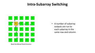
- 19. Intra-Subarray Switching âĒ Communication within the subarray is simple and takes one clock cycle per LUT evaluation and interconnect. âĒ Once a LUT has all of its inputs loaded, the LUT output can be selected as an input to the crossbar, and the LUT's consumers within the subarray may be selected as crossbar outputs.
- 20. Intra-Subarray Switching âĒ A number of subarray outputs are run to each subarray in the same row and column.