際際滷

際際滷Share a Scribd company logo
Introduction to VLSI
Design
V. Jagathi
M Tech , VLSI DESIGN
SRM University
Overview
 VLSI Overview
 Transistor Structure
 Static CMOS Logic
 VLSI Trends
Objectives
VLSI Circuit Analysis:
 Understand MOS transistor operation, design eqns.
 Understand parasitic & perform simple calculations
 Understand static & dynamic CMOS logic
 Estimate delay of CMOS gates, networks, & long
wires
 Estimate power consumption
 Understand design and operation of latches &
flip/flops
Objectives
 CMOS Processing and Layout
 Understand the VLSI manufacturing process.
 Have an appreciation of current trends in VLSI
manufacturing.
 Understand layout design rules.
 Design and analyze layouts for simple digital CMOS
circuits
 Design and analyze hierarchical circuit layouts.
 Understand ASIC Layout styles.
VLSI Overview
 Why Make IC
 IC Evolution
 Common technologies
 CMOS Transistors & Logic Gates
 Structure
 Switch-Level Transistor Model
 Basic gates
 The VLSI Design Process
 Levels of Abstraction
 Design steps
 Design styles
 VLSI Trends
Why ICs are Important
 Integration improves
 size
 speed
 power
 Integration reduce manufacturing costs
 (almost) no manual assembly
IC Evolution
 SSI  Small Scale Integration (early 1970s)
 contained 1  10 logic gates
 MSI  Medium Scale Integration
 logic functions, counters
 LSI  Large Scale Integration
 first microprocessors on the chip
 VLSI  Very Large Scale Integration
 now offers 64-bit microprocessors,
complete with cache memory (L1 and often L2),
floating-point arithmetic unit(s), etc.
IC Evolution
 Bipolar technology
 TTL (transistor-transistor logic)
 ECL (emitter-coupled logic)
 MOS (Metal-oxide-silicon)
 although invented before bipolar transistor,
was initially difficult to manufacture
 nMOS (n-channel MOS) technology developed in
1970s
required fewer masking steps, was denser, and
consumed less power than equivalent bipolar ICs.
IC Evolution
 aluminum gates for replaced by polysilicon by early
1980
 CMOS (Complementary MOS): n-channel and p-
channel MOS transistors =>
lower power consumption, simplified fabrication
process
 Bi-CMOS - hybrid Bipolar, CMOS (for high
speed)
 GaAs - Gallium Arsenide (for high speed)
 Si-Ge - Silicon Germanium (for RF)
Silicon Manufacturing
Alternatives
Standard Components Application Specific ICs
Fixed
Application
Application
by Programming
Semi
Custom
Silicon
Compilation
Full
Custom
Logic
Families
Hardware
Programming
(MASK)
Software
Programming
TTL
CMOS
PLA
ROM
Microprocessor
EPROM,EEPROM
PLD
VLSI Technology - CMOS
Transistors
Key feature:
transistor length L
p+ p+
n substrate
channel
Source Drain
p transistor
G
S
D
SB
Polysilicon Gate
SiO 2
Insulator L
W
G
substrate connected
to VDD
Polysilicon Gate
SiO 2
Insulator
n+ n+
p substrate
channel
Source Drain
n transistor
G
S
D
SB
L
W
G
S
D
substrate connected
to GND
2002: L=130nm
2003: L=90nm
2005: L=65nm?
Transistor Switch Model
 NFET or n transistor
 on when gate H
 "good" switch for logic L
 "poor" switch for logic H
 "pull-down" device
 PFET or p transistor
 on when gate L
 "good" switch for logic H
 "poor" switch for logic L
 "pull-up" device
L H
L L
L L
H L
H H
OFF
when gate=L
ON
when gate=H
OFF
when gate=H
ON
when gate=L
CMOS Logic Design
 Complementary transistor networks
 Pullup: p transistors
 Pulldown - n transistors
VDD
Out
Gnd
VDD
Out
Gnd
Pullup
Network
(p-transistors)
Pulldown
Network
(n-transistors)
InInputs
Inverter
CMOS Inverter Operation
V DD
L
Gnd
H
O N
O FF
V DD
H
Gnd
L
O FF
O N
CMOS Logic Example
A B
A
B
O UT
+V DD
GND
P Transistors
on when gate L
N Transistors
on when gate H
A
B
O UT
NA ND
VLSI Levels of Abstraction
Specification
(what the chip does, inputs/outputs)
Architecture
major resources, connections
Register-Transfer
logic blocks, FSMs, connections
Circuit
transistors, parasitics, connections
Layout
mask layers, polygons
Logic
gates, flip-flops, latches, connections
The VLSI Design Process
 Move from higher to lower levels of abstraction
 Use CAD tools to automate parts of the process
 Use hierarchy to manage complexity
 Different design styles trade off:
Design time
Non-recurring engineering (NRE) cost
Unit cost
Performance
Power Consumption
VLSI Design Tradeoffs
 Non-Recurring Engineering (NRE) Costs
Design Costs
Mask Tooling costs
 Unit Cost - related to chip size
Amount of logic
Current technology
 Performance
Clock speed
Implementation
VLSI Design Tradeoffs
 Power consumption - a relatively new concern
 Power supply voltage
 Clock speed
VLSI Design Styles
 Full Custom
 Application-Specific Integrated Circuit (ASIC)
 Programmable Logic (PLD, FPGA)
 System-on-a-Chip
Full Custom Design
 Each circuit element carefully handcrafted
 Huge design effort
 High Design & NRE Costs / Low Unit Cost
 High Performance
 Typically used for high-volume applications
Application-Specific Integrated
Circuit (ASIC)
 Constrained design using pre-designed (and
sometimes pre-manufactured) components
 Also called semi-custom design
 CAD tools greatly reduce design effort
 Low Design Cost / High NRE Cost / Med.
Unit Cost
 Medium Performance
Programmable Logic (PLDs,
FPGAs)
 Pre-manufactured components with
programmable interconnect
 CAD tools greatly reduce design effort
 Low Design Cost / Low NRE Cost / High Unit
Cost
 Lower Performance
System-on-a-chip (SOC)
 Idea: combine several large blocks
 Predesigned custom cores (e.g., microcontroller)
- intellectual property (IP)
 ASIC logic for special-purpose hardware
 Programmable Logic (PLD, FPGA)
 Analog
 Open issues
 Keeping design cost low
 Verifying correctness of design
Microprocessor Trends (Intel)
Y e ar Chip L transistors
1971 4004 10袖m 2.3K
1974 8080 6袖m 6.0K
1976 8088 3袖m 29K
1982 80286 1.5袖m 134K
1985 80386 1.5袖m 275K
1989 80486 0.8袖m 1.2M
1993 Pe ntium速 0.8袖m 3.1M
1995 Pe ntium速 Pro 0.6袖m 15.5M
1999 Mobile PII 0.25袖m 27.4
2000 Pe ntium速 4 0.18袖m 42M
2002 Pe ntium速 4 (N) 0.13袖m 55M
Source: http://www.intel.com/pressroom/kits/quickreffam.htm
Trends in VLSI
 Transistor
Smaller, faster, use less power
 Interconnect
Less resistive, faster, longer (denser
design)
 Yield
Smaller die size, higher yield
Power and Noise
 Huge power consumption and heat
dissipation becomes a problem
 Noise and cross talk.
 Solutions:
Better physical design
Interconnect Delay
 Interconnect delay becomes a dominating
factor in circuit performance
 Solutions:
Use copper wire
Interconnect optimization in physical
design, e.g., wire sizing, buffer insertion,
buffer sizing.
Interconnect Delay
0.65
1989
0.5
1992
0.35
1995
0.25
1998
0.18
2001
0.13
2004
0.1
2007
0
5
10
15
20
25
30
35
40
Gate delay
Interconnect delay
Source: SIA Roadmap 1997
vlsi

More Related Content

What's hot (20)

Design of ring oscillator using controlled low voltage swing inverter
Design of ring oscillator using controlled low voltage swing inverter Design of ring oscillator using controlled low voltage swing inverter
Design of ring oscillator using controlled low voltage swing inverter
khush_19
Vlsi physical design
Vlsi physical designVlsi physical design
Vlsi physical design
I World Tech
Fpga in space
Fpga in spaceFpga in space
Fpga in space
JBPooMahaVinuShree
Digital VLSI Design : Introduction
Digital VLSI Design : IntroductionDigital VLSI Design : Introduction
Digital VLSI Design : Introduction
Usha Mehta
Placement and routing in full custom physical design
Placement and routing in full custom physical designPlacement and routing in full custom physical design
Placement and routing in full custom physical design
Deiptii Das
Vlsi technology-dinesh
Vlsi technology-dineshVlsi technology-dinesh
Vlsi technology-dinesh
dinesh kumar
Multi mode multi corner (mmmc)
Multi mode multi corner (mmmc)Multi mode multi corner (mmmc)
Multi mode multi corner (mmmc)
shaik sharief
Basic synthesis flow and commands in digital VLSI
Basic synthesis flow and commands in digital VLSIBasic synthesis flow and commands in digital VLSI
Basic synthesis flow and commands in digital VLSI
Surya Raj
Vlsi physical design automation on partitioning
Vlsi physical design automation on partitioningVlsi physical design automation on partitioning
Vlsi physical design automation on partitioning
Sushil Kundu
Verilog Test Bench
Verilog Test BenchVerilog Test Bench
Verilog Test Bench
Dr.YNM
Introduction to VLSI
Introduction to VLSI Introduction to VLSI
Introduction to VLSI
illpa
Soc architecture and design
Soc architecture and designSoc architecture and design
Soc architecture and design
Satya Harish
Clk-to-q delay, library setup and hold time
Clk-to-q delay, library setup and hold timeClk-to-q delay, library setup and hold time
Clk-to-q delay, library setup and hold time
VLSI SYSTEM Design
Morello Technology Demonstrator Hardware Overview - Mark Inskip, Arm
Morello Technology Demonstrator Hardware Overview - Mark Inskip, ArmMorello Technology Demonstrator Hardware Overview - Mark Inskip, Arm
Morello Technology Demonstrator Hardware Overview - Mark Inskip, Arm
KTN
High efficiency power amplifiers
High efficiency power amplifiersHigh efficiency power amplifiers
High efficiency power amplifiers
Abhishek Kadam
VLSI technology
VLSI technologyVLSI technology
VLSI technology
Aidell2583
Catalog Feeo Solar
Catalog Feeo SolarCatalog Feeo Solar
Catalog Feeo Solar
HUY HOANG TECHNOLOGY JOINT STOCK COMPANY
SISTec Microelectronics VLSI design
SISTec Microelectronics VLSI designSISTec Microelectronics VLSI design
SISTec Microelectronics VLSI design
Dr. Ravi Mishra
Implementing Useful Clock Skew Using Skew Groups
Implementing Useful Clock Skew Using Skew GroupsImplementing Useful Clock Skew Using Skew Groups
Implementing Useful Clock Skew Using Skew Groups
M Mei
VLSI UNIT-1.1.pdf.ppt
VLSI UNIT-1.1.pdf.pptVLSI UNIT-1.1.pdf.ppt
VLSI UNIT-1.1.pdf.ppt
rajukolluri
Design of ring oscillator using controlled low voltage swing inverter
Design of ring oscillator using controlled low voltage swing inverter Design of ring oscillator using controlled low voltage swing inverter
Design of ring oscillator using controlled low voltage swing inverter
khush_19
Vlsi physical design
Vlsi physical designVlsi physical design
Vlsi physical design
I World Tech
Digital VLSI Design : Introduction
Digital VLSI Design : IntroductionDigital VLSI Design : Introduction
Digital VLSI Design : Introduction
Usha Mehta
Placement and routing in full custom physical design
Placement and routing in full custom physical designPlacement and routing in full custom physical design
Placement and routing in full custom physical design
Deiptii Das
Vlsi technology-dinesh
Vlsi technology-dineshVlsi technology-dinesh
Vlsi technology-dinesh
dinesh kumar
Multi mode multi corner (mmmc)
Multi mode multi corner (mmmc)Multi mode multi corner (mmmc)
Multi mode multi corner (mmmc)
shaik sharief
Basic synthesis flow and commands in digital VLSI
Basic synthesis flow and commands in digital VLSIBasic synthesis flow and commands in digital VLSI
Basic synthesis flow and commands in digital VLSI
Surya Raj
Vlsi physical design automation on partitioning
Vlsi physical design automation on partitioningVlsi physical design automation on partitioning
Vlsi physical design automation on partitioning
Sushil Kundu
Verilog Test Bench
Verilog Test BenchVerilog Test Bench
Verilog Test Bench
Dr.YNM
Introduction to VLSI
Introduction to VLSI Introduction to VLSI
Introduction to VLSI
illpa
Soc architecture and design
Soc architecture and designSoc architecture and design
Soc architecture and design
Satya Harish
Clk-to-q delay, library setup and hold time
Clk-to-q delay, library setup and hold timeClk-to-q delay, library setup and hold time
Clk-to-q delay, library setup and hold time
VLSI SYSTEM Design
Morello Technology Demonstrator Hardware Overview - Mark Inskip, Arm
Morello Technology Demonstrator Hardware Overview - Mark Inskip, ArmMorello Technology Demonstrator Hardware Overview - Mark Inskip, Arm
Morello Technology Demonstrator Hardware Overview - Mark Inskip, Arm
KTN
High efficiency power amplifiers
High efficiency power amplifiersHigh efficiency power amplifiers
High efficiency power amplifiers
Abhishek Kadam
VLSI technology
VLSI technologyVLSI technology
VLSI technology
Aidell2583
SISTec Microelectronics VLSI design
SISTec Microelectronics VLSI designSISTec Microelectronics VLSI design
SISTec Microelectronics VLSI design
Dr. Ravi Mishra
Implementing Useful Clock Skew Using Skew Groups
Implementing Useful Clock Skew Using Skew GroupsImplementing Useful Clock Skew Using Skew Groups
Implementing Useful Clock Skew Using Skew Groups
M Mei
VLSI UNIT-1.1.pdf.ppt
VLSI UNIT-1.1.pdf.pptVLSI UNIT-1.1.pdf.ppt
VLSI UNIT-1.1.pdf.ppt
rajukolluri

Viewers also liked (9)

Ic tech unit 5- VLSI Process Integration
Ic tech unit 5- VLSI Process IntegrationIc tech unit 5- VLSI Process Integration
Ic tech unit 5- VLSI Process Integration
kriticka sharma
CMOS Topic 6 -_designing_combinational_logic_circuits
CMOS Topic 6 -_designing_combinational_logic_circuitsCMOS Topic 6 -_designing_combinational_logic_circuits
CMOS Topic 6 -_designing_combinational_logic_circuits
Ikhwan_Fakrudin
9.sequential+circuits part+1
9.sequential+circuits part+1 9.sequential+circuits part+1
9.sequential+circuits part+1
liran1018
IS 151 Lecture 9
IS 151 Lecture 9IS 151 Lecture 9
IS 151 Lecture 9
wajanga
Vlsi design mosfet
Vlsi design mosfetVlsi design mosfet
Vlsi design mosfet
vennila12
Lecture11 combinational logic dynamics
Lecture11 combinational logic dynamicsLecture11 combinational logic dynamics
Lecture11 combinational logic dynamics
vidhya DS
Pass Transistor Logic
Pass Transistor LogicPass Transistor Logic
Pass Transistor Logic
Diwaker Pant
Analog vlsi
Analog vlsiAnalog vlsi
Analog vlsi
Khuong Lamborghini
Pass transistor logic
Pass transistor logicPass transistor logic
Pass transistor logic
Tripurna Chary
Ic tech unit 5- VLSI Process Integration
Ic tech unit 5- VLSI Process IntegrationIc tech unit 5- VLSI Process Integration
Ic tech unit 5- VLSI Process Integration
kriticka sharma
CMOS Topic 6 -_designing_combinational_logic_circuits
CMOS Topic 6 -_designing_combinational_logic_circuitsCMOS Topic 6 -_designing_combinational_logic_circuits
CMOS Topic 6 -_designing_combinational_logic_circuits
Ikhwan_Fakrudin
9.sequential+circuits part+1
9.sequential+circuits part+1 9.sequential+circuits part+1
9.sequential+circuits part+1
liran1018
IS 151 Lecture 9
IS 151 Lecture 9IS 151 Lecture 9
IS 151 Lecture 9
wajanga
Vlsi design mosfet
Vlsi design mosfetVlsi design mosfet
Vlsi design mosfet
vennila12
Lecture11 combinational logic dynamics
Lecture11 combinational logic dynamicsLecture11 combinational logic dynamics
Lecture11 combinational logic dynamics
vidhya DS
Pass Transistor Logic
Pass Transistor LogicPass Transistor Logic
Pass Transistor Logic
Diwaker Pant
Pass transistor logic
Pass transistor logicPass transistor logic
Pass transistor logic
Tripurna Chary

Similar to vlsi (20)

Semiconductor overview
Semiconductor overviewSemiconductor overview
Semiconductor overview
Nabil Chouba
VLSI unit 1 Technology - S.ppt
VLSI unit 1 Technology - S.pptVLSI unit 1 Technology - S.ppt
VLSI unit 1 Technology - S.ppt
indrajeetPatel22
My profile
My profileMy profile
My profile
dhruv_63
Chapter_01 Course Introduction.pdf
Chapter_01 Course Introduction.pdfChapter_01 Course Introduction.pdf
Chapter_01 Course Introduction.pdf
VoThanhPhong3
VLSI Design- Guru.ppt
VLSI Design- Guru.pptVLSI Design- Guru.ppt
VLSI Design- Guru.ppt
Ram Pavithra Guru
vlsi fabrication technology scheme20.pdf
vlsi fabrication technology scheme20.pdfvlsi fabrication technology scheme20.pdf
vlsi fabrication technology scheme20.pdf
KalluruChintu
vlsi fabrication technology scheme20.pdf
vlsi fabrication technology scheme20.pdfvlsi fabrication technology scheme20.pdf
vlsi fabrication technology scheme20.pdf
KalluruChintu
Introduction to EDA Tools
Introduction to EDA ToolsIntroduction to EDA Tools
Introduction to EDA Tools
venkatasuman1983
Implementation strategies for digital ics
Implementation strategies for digital icsImplementation strategies for digital ics
Implementation strategies for digital ics
aroosa khan
Very Large Scale Integrated Circuits VLSI Overview
Very Large Scale Integrated Circuits VLSI OverviewVery Large Scale Integrated Circuits VLSI Overview
Very Large Scale Integrated Circuits VLSI Overview
Engr. Bilal Sarwar
Resume
ResumeResume
Resume
jaydippatel
L1 introduction
L1 introductionL1 introduction
L1 introduction
pooja bagde
Asic
AsicAsic
Asic
rajeevkr35
Unit-4_ESE.pdf
Unit-4_ESE.pdfUnit-4_ESE.pdf
Unit-4_ESE.pdf
SouravRoyElectronics
1st and 2nd Lecture
1st and 2nd Lecture1st and 2nd Lecture
1st and 2nd Lecture
babak danyal
Asic design lect1 2 august 28 2012
Asic design lect1 2 august 28 2012Asic design lect1 2 august 28 2012
Asic design lect1 2 august 28 2012
babak danyal
Hard IP Core design | Convolution Encoder
Hard IP Core design | Convolution EncoderHard IP Core design | Convolution Encoder
Hard IP Core design | Convolution Encoder
Archit Vora
Introduction to VLSI
Introduction to VLSIIntroduction to VLSI
Introduction to VLSI
Shams Tabrej
M Tech New Syllabus(2012)
M Tech New Syllabus(2012)M Tech New Syllabus(2012)
M Tech New Syllabus(2012)
BGS Institute of Technology, Adichunchanagiri University (ACU)
Lecture20 asic back_end_design
Lecture20 asic back_end_designLecture20 asic back_end_design
Lecture20 asic back_end_design
Hung Nguyen
Semiconductor overview
Semiconductor overviewSemiconductor overview
Semiconductor overview
Nabil Chouba
VLSI unit 1 Technology - S.ppt
VLSI unit 1 Technology - S.pptVLSI unit 1 Technology - S.ppt
VLSI unit 1 Technology - S.ppt
indrajeetPatel22
My profile
My profileMy profile
My profile
dhruv_63
Chapter_01 Course Introduction.pdf
Chapter_01 Course Introduction.pdfChapter_01 Course Introduction.pdf
Chapter_01 Course Introduction.pdf
VoThanhPhong3
vlsi fabrication technology scheme20.pdf
vlsi fabrication technology scheme20.pdfvlsi fabrication technology scheme20.pdf
vlsi fabrication technology scheme20.pdf
KalluruChintu
vlsi fabrication technology scheme20.pdf
vlsi fabrication technology scheme20.pdfvlsi fabrication technology scheme20.pdf
vlsi fabrication technology scheme20.pdf
KalluruChintu
Introduction to EDA Tools
Introduction to EDA ToolsIntroduction to EDA Tools
Introduction to EDA Tools
venkatasuman1983
Implementation strategies for digital ics
Implementation strategies for digital icsImplementation strategies for digital ics
Implementation strategies for digital ics
aroosa khan
Very Large Scale Integrated Circuits VLSI Overview
Very Large Scale Integrated Circuits VLSI OverviewVery Large Scale Integrated Circuits VLSI Overview
Very Large Scale Integrated Circuits VLSI Overview
Engr. Bilal Sarwar
L1 introduction
L1 introductionL1 introduction
L1 introduction
pooja bagde
1st and 2nd Lecture
1st and 2nd Lecture1st and 2nd Lecture
1st and 2nd Lecture
babak danyal
Asic design lect1 2 august 28 2012
Asic design lect1 2 august 28 2012Asic design lect1 2 august 28 2012
Asic design lect1 2 august 28 2012
babak danyal
Hard IP Core design | Convolution Encoder
Hard IP Core design | Convolution EncoderHard IP Core design | Convolution Encoder
Hard IP Core design | Convolution Encoder
Archit Vora
Introduction to VLSI
Introduction to VLSIIntroduction to VLSI
Introduction to VLSI
Shams Tabrej
Lecture20 asic back_end_design
Lecture20 asic back_end_designLecture20 asic back_end_design
Lecture20 asic back_end_design
Hung Nguyen

vlsi

  • 1. Introduction to VLSI Design V. Jagathi M Tech , VLSI DESIGN SRM University
  • 2. Overview VLSI Overview Transistor Structure Static CMOS Logic VLSI Trends
  • 3. Objectives VLSI Circuit Analysis: Understand MOS transistor operation, design eqns. Understand parasitic & perform simple calculations Understand static & dynamic CMOS logic Estimate delay of CMOS gates, networks, & long wires Estimate power consumption Understand design and operation of latches & flip/flops
  • 4. Objectives CMOS Processing and Layout Understand the VLSI manufacturing process. Have an appreciation of current trends in VLSI manufacturing. Understand layout design rules. Design and analyze layouts for simple digital CMOS circuits Design and analyze hierarchical circuit layouts. Understand ASIC Layout styles.
  • 5. VLSI Overview Why Make IC IC Evolution Common technologies CMOS Transistors & Logic Gates Structure Switch-Level Transistor Model Basic gates The VLSI Design Process Levels of Abstraction Design steps Design styles VLSI Trends
  • 6. Why ICs are Important Integration improves size speed power Integration reduce manufacturing costs (almost) no manual assembly
  • 7. IC Evolution SSI Small Scale Integration (early 1970s) contained 1 10 logic gates MSI Medium Scale Integration logic functions, counters LSI Large Scale Integration first microprocessors on the chip VLSI Very Large Scale Integration now offers 64-bit microprocessors, complete with cache memory (L1 and often L2), floating-point arithmetic unit(s), etc.
  • 8. IC Evolution Bipolar technology TTL (transistor-transistor logic) ECL (emitter-coupled logic) MOS (Metal-oxide-silicon) although invented before bipolar transistor, was initially difficult to manufacture nMOS (n-channel MOS) technology developed in 1970s required fewer masking steps, was denser, and consumed less power than equivalent bipolar ICs.
  • 9. IC Evolution aluminum gates for replaced by polysilicon by early 1980 CMOS (Complementary MOS): n-channel and p- channel MOS transistors => lower power consumption, simplified fabrication process Bi-CMOS - hybrid Bipolar, CMOS (for high speed) GaAs - Gallium Arsenide (for high speed) Si-Ge - Silicon Germanium (for RF)
  • 10. Silicon Manufacturing Alternatives Standard Components Application Specific ICs Fixed Application Application by Programming Semi Custom Silicon Compilation Full Custom Logic Families Hardware Programming (MASK) Software Programming TTL CMOS PLA ROM Microprocessor EPROM,EEPROM PLD
  • 11. VLSI Technology - CMOS Transistors Key feature: transistor length L p+ p+ n substrate channel Source Drain p transistor G S D SB Polysilicon Gate SiO 2 Insulator L W G substrate connected to VDD Polysilicon Gate SiO 2 Insulator n+ n+ p substrate channel Source Drain n transistor G S D SB L W G S D substrate connected to GND 2002: L=130nm 2003: L=90nm 2005: L=65nm?
  • 12. Transistor Switch Model NFET or n transistor on when gate H "good" switch for logic L "poor" switch for logic H "pull-down" device PFET or p transistor on when gate L "good" switch for logic H "poor" switch for logic L "pull-up" device L H L L L L H L H H OFF when gate=L ON when gate=H OFF when gate=H ON when gate=L
  • 13. CMOS Logic Design Complementary transistor networks Pullup: p transistors Pulldown - n transistors VDD Out Gnd VDD Out Gnd Pullup Network (p-transistors) Pulldown Network (n-transistors) InInputs Inverter
  • 14. CMOS Inverter Operation V DD L Gnd H O N O FF V DD H Gnd L O FF O N
  • 15. CMOS Logic Example A B A B O UT +V DD GND P Transistors on when gate L N Transistors on when gate H A B O UT NA ND
  • 16. VLSI Levels of Abstraction Specification (what the chip does, inputs/outputs) Architecture major resources, connections Register-Transfer logic blocks, FSMs, connections Circuit transistors, parasitics, connections Layout mask layers, polygons Logic gates, flip-flops, latches, connections
  • 17. The VLSI Design Process Move from higher to lower levels of abstraction Use CAD tools to automate parts of the process Use hierarchy to manage complexity Different design styles trade off: Design time Non-recurring engineering (NRE) cost Unit cost Performance Power Consumption
  • 18. VLSI Design Tradeoffs Non-Recurring Engineering (NRE) Costs Design Costs Mask Tooling costs Unit Cost - related to chip size Amount of logic Current technology Performance Clock speed Implementation
  • 19. VLSI Design Tradeoffs Power consumption - a relatively new concern Power supply voltage Clock speed
  • 20. VLSI Design Styles Full Custom Application-Specific Integrated Circuit (ASIC) Programmable Logic (PLD, FPGA) System-on-a-Chip
  • 21. Full Custom Design Each circuit element carefully handcrafted Huge design effort High Design & NRE Costs / Low Unit Cost High Performance Typically used for high-volume applications
  • 22. Application-Specific Integrated Circuit (ASIC) Constrained design using pre-designed (and sometimes pre-manufactured) components Also called semi-custom design CAD tools greatly reduce design effort Low Design Cost / High NRE Cost / Med. Unit Cost Medium Performance
  • 23. Programmable Logic (PLDs, FPGAs) Pre-manufactured components with programmable interconnect CAD tools greatly reduce design effort Low Design Cost / Low NRE Cost / High Unit Cost Lower Performance
  • 24. System-on-a-chip (SOC) Idea: combine several large blocks Predesigned custom cores (e.g., microcontroller) - intellectual property (IP) ASIC logic for special-purpose hardware Programmable Logic (PLD, FPGA) Analog Open issues Keeping design cost low Verifying correctness of design
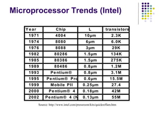
  • 25. Microprocessor Trends (Intel) Y e ar Chip L transistors 1971 4004 10袖m 2.3K 1974 8080 6袖m 6.0K 1976 8088 3袖m 29K 1982 80286 1.5袖m 134K 1985 80386 1.5袖m 275K 1989 80486 0.8袖m 1.2M 1993 Pe ntium速 0.8袖m 3.1M 1995 Pe ntium速 Pro 0.6袖m 15.5M 1999 Mobile PII 0.25袖m 27.4 2000 Pe ntium速 4 0.18袖m 42M 2002 Pe ntium速 4 (N) 0.13袖m 55M Source: http://www.intel.com/pressroom/kits/quickreffam.htm
  • 26. Trends in VLSI Transistor Smaller, faster, use less power Interconnect Less resistive, faster, longer (denser design) Yield Smaller die size, higher yield
  • 27. Power and Noise Huge power consumption and heat dissipation becomes a problem Noise and cross talk. Solutions: Better physical design
  • 28. Interconnect Delay Interconnect delay becomes a dominating factor in circuit performance Solutions: Use copper wire Interconnect optimization in physical design, e.g., wire sizing, buffer insertion, buffer sizing.