


![[Giao trinh] vi dieu-khien_8051 - dh tra vinh](https://cdn.slidesharecdn.com/ss_thumbnails/giaotrinh-vidieukhien8051-dhtravinh-140114075729-phpapp02-thumbnail.jpg?width=560&fit=bounds)


More Related Content
What's hot (20)
Similar to Vxl ch03-8051-3.1 3.2-v03 (20)


More from Huynh MVT (20)


Recently uploaded (18)
![[PPT11] B├Āi 7 - ─Éß╗Źc - C├Ā Mau qu├¬ xß╗®.pptx](https://cdn.slidesharecdn.com/ss_thumbnails/ppt11bi7-c-cmauqux-250305070313-62766c8d-thumbnail.jpg?width=560&fit=bounds)


![[PPT11] B├Āi 7 - ─Éß╗Źc - V├Ā t├┤i vß║½n muß╗æn mß║╣....ppt](https://cdn.slidesharecdn.com/ss_thumbnails/ppt11bi7-c-vtivnmunm-250305063122-6e221a47-thumbnail.jpg?width=560&fit=bounds)
Vxl ch03-8051-3.1 3.2-v03
- 1. Hß╗ī VI ─ÉIß╗ĆU KHIß╗éN 8051 1 Hiß╗ću ─æ├Łnh tß╗½ slide cß╗¦a thß║¦y Hß╗ō Trung Mß╗╣ Bß╗Ö m├┤n ─Éiß╗ćn tß╗Ł - DH BK TPHCM
- 2. Nß╗Öi dung 3.1 Giß╗øi thiß╗ću hß╗Ź vi ─æiß╗üu khiß╗ān 8051 3.2 Kiß║┐n tr├║c phß║¦n cß╗®ng 8051 2
- 3. 3.1 Giß╗øi thiß╗ću hß╗Ź vi ─æiß╗üu khiß╗ān 8051 3
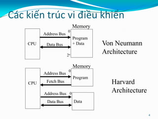
- 4. C├Īc kiß║┐n tr├║c vi ─æiß╗üu khiß╗ān 4 CPU Program + Data Address Bus Data Bus Memory Von Neumann Architecture CPU Program Address Bus Data Bus Harvard Architecture Memory Data Address Bus Fetch Bus 0 0 0 2n
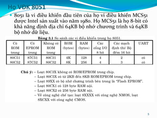
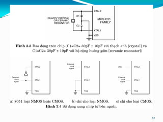
- 5. Hß╗Ź V─ÉK 8051 ’éŚ 8051 l├Ā vi ─æiß╗üu khiß╗ān ─æß║¦u ti├¬n cß╗¦a hß╗Ź vi ─æiß╗üu khiß╗ān MCS51 ─æŲ░ß╗Żc Intel sß║Żn xuß║źt v├Āo n─ām 1980. Hß╗Ź MCS51 l├Ā hß╗Ź 8-bit c├│ khß║Ż n─āng ─æß╗ŗnh ─æß╗ŗa chß╗ē 64KB bß╗Ö nhß╗ø chŲ░ŲĪng tr├¼nh v├Ā 64KB bß╗Ö nhß╗ø dß╗» liß╗ću. 5
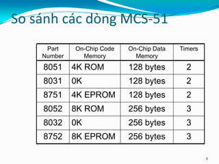
- 6. So So s├Īnh s├Īnh c├Īc c├Īc d├▓ng d├▓ng MCS MCS- -51 51 6 3 256 bytes 8K EPROM 8752 3 256 bytes 0K 8032 3 256 bytes 8K ROM 8052 2 128 bytes 4K EPROM 8751 2 128 bytes 0K 8031 2 128 bytes 4K ROM 8051 Timers On-Chip Data Memory On-Chip Code Memory Part Number
- 7. 3.2 Kiß║┐n tr├║c phß║¦n cß╗®ng 8051 7
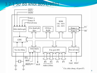
- 8. 3.2.1 SŲĪ ─æß╗ō khß╗æi 8051/8031 8
- 9. 9
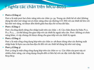
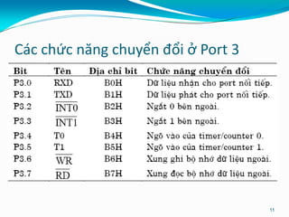
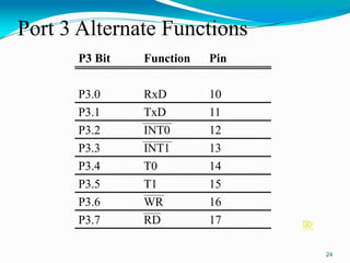
- 10. ├Ø ngh─®a c├Īc ch├ón tr├¬n MCU 8051 ’éŚ Port 0 (Cß╗Ģng 0) Port 0 l├Ā mß╗Öt port hai chß╗®c n─āng tr├¬n c├Īc ch├ón 32ŌĆō39. Trong c├Īc thiß║┐t kß║┐ cß╗Ī nhß╗Å (kh├┤ng d├╣ng bß╗Ö nhß╗ø mß╗¤ rß╗Öng) n├│ c├│ chß╗®c n─āng nhŲ░ c├Īc ─æŲ░ß╗Øng I/O. ─Éß╗æi vß╗øi c├Īc thiß║┐t kß║┐ lß╗øn vß╗øi bß╗Ö nhß╗ø mß╗¤ rß╗Öng, n├│ ─æŲ░ß╗Żc dß╗ōn k├¬nh giß╗»a bus ─æß╗ŗa chß╗ē v├Ā bus dß╗» liß╗ću. ’éŚ Port 1 (Cß╗Ģng 1) Port 1 l├Ā cß╗Ģng d├Ānh ri├¬ng cho nhß║Łp/xuß║źt tr├¬n c├Īc ch├ón 1ŌĆō8. C├Īc ch├ón ─æŲ░ß╗Żc k├Į hiß╗ću P1.0, P1.1, P1.2, ... c├│ thß╗ā d├╣ng cho giao tiß║┐p vß╗øi c├Īc thiß║┐t bß╗ŗ ngo├Āi nß║┐u cß║¦n. Port 1 kh├┤ng c├│ chß╗®c n─āng kh├Īc, v├¼ vß║Ły ch├║ng chß╗ē ─æŲ░ß╗Żc d├╣ng cho giao tiß║┐p vß╗øi c├Īc thiß║┐t bß╗ŗ ngo├Āi. ’éŚ Port 2 (Cß╗Ģng 2) Port 2 l├Ā mß╗Öt cß╗Ģng c├┤ng dß╗źng k├®p tr├¬n c├Īc ch├ón 21ŌĆō28 ─æŲ░ß╗Żc d├╣ng nhŲ░ c├Īc ─æŲ░ß╗Øng xuß║źt nhß║Łp hoß║Ęc l├Ā byte cao cß╗¦a bus ─æß╗ŗa chß╗ē ─æß╗æi vß╗øi c├Īc thiß║┐t kß║┐ d├╣ng bß╗Ö nhß╗ø mß╗¤ rß╗Öng. ’éŚ Port 3 (Cß╗Ģng 3) Port 3 c┼®ng l├Ā mß╗Öt cß╗Ģng c├┤ng dß╗źng k├®p tr├¬n c├Īc ch├ón 10ŌĆō17. C├Īc ch├ón cß╗¦a port n├Āy c├│ nhiß╗üu chß╗®c n─āng, c├Īc c├┤ng dß╗źng chuyß╗ān ─æß╗Ģi c├│ li├¬n hß╗ć vß╗øi c├Īc ─æß║Ęc t├Łnh ─æß║Ęc biß╗ćt cß╗¦a 8051/8031 10
- 11. C├Īc chß╗®c n─āng chuyß╗ān ─æß╗Ģi ß╗¤ Port 3 11
- 12. 12
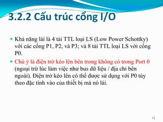
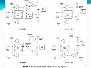
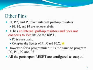
- 13. 3.2.2 Cß║źu tr├║c cß╗Ģng I/O ’éŚ Khß║Ż n─āng l├Īi l├Ā 4 tß║Żi TTL loß║Īi LS (Low Power Schottky) vß╗øi c├Īc cß╗Ģng P1, P2, v├Ā P3; v├Ā 8 tß║Żi TTL loß║Īi LS vß╗øi cß╗Ģng P0. ’éŚ Ch├║ ├Į l├Ā ─æiß╗ćn trß╗¤ k├®o l├¬n b├¬n trong kh├┤ng c├│ trong Port 0 (ngoß║Īi trß╗½ l├║c l├Ām viß╗ćc nhŲ░ bus dß╗» liß╗ću / ─æß╗ŗa chß╗ē b├¬n ngo├Āi). ─Éiß╗ćn trß╗¤ k├®o l├¬n c├│ thß╗ā ─æŲ░ß╗Żc sß╗Ł dß╗źng vß╗øi P0 t├╣y theo ─æß║Ęc t├Łnh v├Āo cß╗¦a thiß║┐t bß╗ŗ m├Ā n├│ l├Īi. 13
- 14. 14
- 15. 15
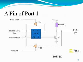
- 16. A Pin of Port 1 16 8051 IC D Q Clk Q Vcc Load(L1) Read latch Read pin Write to latch Internal CPU bus M1 P1.X pin P1.X TB1 TB2 ’ā¢P0.x
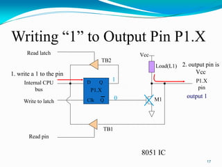
- 17. Writing ŌĆ£1ŌĆØ to Output Pin P1.X 17 D Q Clk Q Vcc Load(L1) Read latch Read pin Write to latch Internal CPU bus M1 P1.X pin P1.X 8051 IC 2. output pin is Vcc 1. write a 1 to the pin 1 0 output 1 TB1 TB2
- 18. Writing ŌĆ£0ŌĆØ to Output Pin P1.X 18 D Q Clk Q Vcc Load(L1) Read latch Read pin Write to latch Internal CPU bus M1 P1.X pin P1.X 8051 IC 2. output pin is ground 1. write a 0 to the pin 0 1 output 0 TB1 TB2
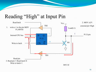
- 19. Reading ŌĆ£HighŌĆØ at Input Pin 19 D Q Clk Q Vcc Load(L1) Read latch Read pin Write to latch Internal CPU bus M1 P1.X pin P1.X 8051 IC 2. MOV A,P1 external pin=High 1. write a 1 to the pin MOV P1,#0FFH 1 0 3. Read pin=1 Read latch=0 Write to latch=1 1 TB1 TB2
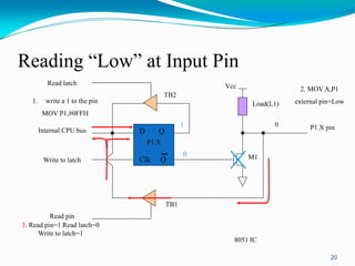
- 20. Reading ŌĆ£LowŌĆØ at Input Pin 20 D Q Clk Q Vcc Load(L1) Read latch Read pin Write to latch Internal CPU bus M1 P1.X pin P1.X 8051 IC 2. MOV A,P1 external pin=Low 1. write a 1 to the pin MOV P1,#0FFH 1 0 3. Read pin=1 Read latch=0 Write to latch=1 0 TB1 TB2
- 21. Other Pins ’éŚ P1, P2, and P3 have internal pull-up resisters. ’éŚ P1, P2, and P3 are not open drain. ’éŚ P0 has no internal pull-up resistors and does not connects to Vcc inside the 8051. ’éŚ P0 is open drain. ’éŚ Compare the figures of P1.X and P0.X. ’ĆĮ ’éŚ However, for a programmer, it is the same to program P0, P1, P2 and P3. ’éŚ All the ports upon RESET are configured as output. 21
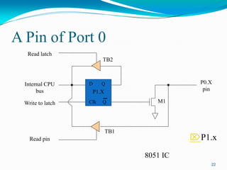
- 22. A Pin of Port 0 22 8051 IC D Q Clk Q Read latch Read pin Write to latch Internal CPU bus M1 P0.X pin P1.X TB1 TB2 ’ā¢P1.x
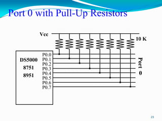
- 23. Port 0 with Pull-Up Resistors 23 P0.0 P0.1 P0.2 P0.3 P0.4 P0.5 P0.6 P0.7 DS5000 8751 8951 Vcc 10 K Port 0
- 24. Port 3 Alternate Functions 24 17 RD P3.7 16 WR P3.6 15 T1 P3.5 14 T0 P3.4 13 INT1 P3.3 12 INT0 P3.2 11 TxD P3.1 10 RxD P3.0 Pin Function P3 Bit ’ā¢
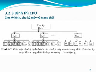
- 25. 3.2.3 ─Éß╗ŗnh th├¼ CPU Chu kß╗│ lß╗ćnh, chu kß╗│ m├Īy v├Ā trß║Īng th├Īi 25
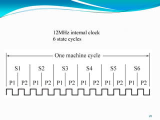
- 26. 12MHz internal clock 6 state cycles 26
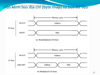
- 27. Dß╗ōn k├¬nh bus ─æß╗ŗa chß╗ē (byte thß║źp) v├Ā bus dß╗» liß╗ću 27
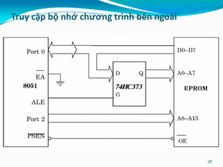
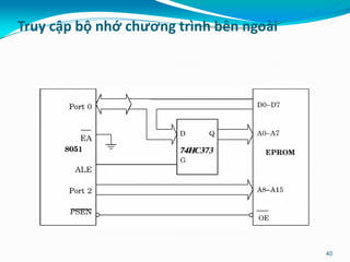
- 28. Truy cß║Łp bß╗Ö nhß╗ø chŲ░ŲĪng tr├¼nh b├¬n ngo├Āi 28
- 29. 29
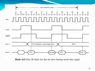
- 30. 30
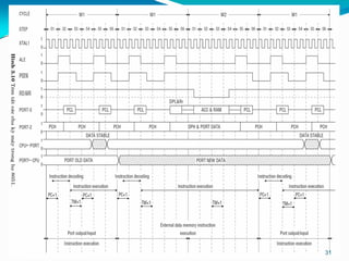
- 31. 31
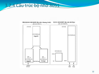
- 32. 3.2.4 Cß║źu tr├║c bß╗Ö nhß╗ø 8051 32
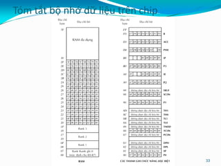
- 33. T├│m tß║»t bß╗Ö nhß╗ø dß╗» liß╗ću tr├¬n chip 33
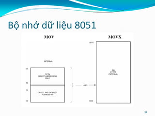
- 34. Bß╗Ö nhß╗ø dß╗» liß╗ću 8051 34
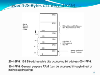
- 35. Lower 128 Bytes of Internal RAM 35 20H-2FH: 128 Bit-addressable bits occupying bit address 00H-7FH. 30H-7FH: General purpose RAM (can be accessed through direct or indirect addressing)
- 36. Upper 128 Bytes of Internal RAM 36
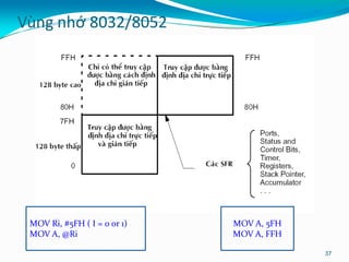
- 37. V├╣ng nhß╗ø 8032/8052 37 MOV A, 5FH MOV A, FFH MOV Ri, #5FH ( I = 0 or 1) MOV A, @Ri
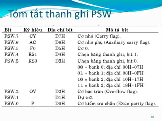
- 38. Tóm tắt thanh ghi PSW 38
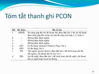
- 39. Tóm tắt thanh ghi PCON 39
- 40. Truy cß║Łp bß╗Ö nhß╗ø chŲ░ŲĪng tr├¼nh b├¬n ngo├Āi 40
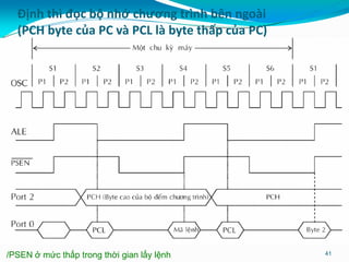
- 41. ─Éß╗ŗnh th├¼ ─æß╗Źc bß╗Ö nhß╗ø chŲ░ŲĪng tr├¼nh b├¬n ngo├Āi (PCH byte cß╗¦a PC v├Ā PCL l├Ā byte thß║źp cß╗¦a PC) 41 /PSEN ß╗¤ mß╗®c thß║źp trong thß╗Øi gian lß║źy lß╗ćnh
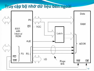
- 42. Truy cß║Łp bß╗Ö nhß╗ø dß╗» liß╗ću b├¬n ngo├Āi 42
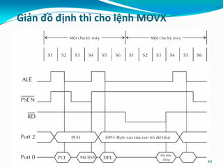
- 43. Giß║Żn ─æß╗ō ─æß╗ŗnh th├¼ cho lß╗ćnh MOVX 43
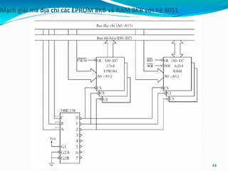
- 44. Mß║Īch giß║Żi m├Ż ─æß╗ŗa chß╗ē c├Īc EPROM 8KB v├Ā RAM 8KB vß╗øi hß╗ć 8051 44
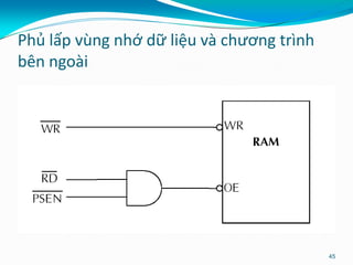
- 45. Phß╗¦ lß║źp v├╣ng nhß╗ø dß╗» liß╗ću v├Ā chŲ░ŲĪng tr├¼nh b├¬n ngo├Āi 45
- 46. 3.2.8 Hoß║Īt ─æß╗Öng reset 46
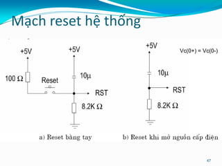
- 47. Mß║Īch reset hß╗ć thß╗æng 47 Vc(0+) = Vc(0-)
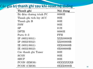
- 48. C├Īc gi├Ī trß╗ŗ thanh ghi sau khi reset hß╗ć thß╗æng 48