![UNIT 4 Syllabus
ïIntroduction: Memory Interfacing & I/O interfacing
âĒ 8255 PPI {Parallel communication interface}
âĒ 8259 {Programmable Interrupt controller }
âĒ 8253/8254 Timer {Timer or counter}
âĒ 8237/8257 {DMA controller}
âĒ 8251 USART {Serial communication interface}
âĒ 8279 {Keyboard /display controller}
âĒ A/D and D/A Interface {ADC 0800/0809,DAC 0800}
[Interfacing with 8085 & 8051]](https://image.slidesharecdn.com/unit-iv-221110133153-af845783/85/Unit-IV-pptx-3-320.jpg)


More Related Content
Similar to Unit-IV.pptx (20)
Recently uploaded (20)


Unit-IV.pptx
- 2. Study on need, Architecture, configuration and interfacing, with ICs: 8255, 8259, 8254, 8279 , A/D and D/A converters & Interfacing with 8085 & 8051.
- 3. UNIT 4 Syllabus ïIntroduction: Memory Interfacing & I/O interfacing âĒ 8255 PPI {Parallel communication interface} âĒ 8259 {Programmable Interrupt controller } âĒ 8253/8254 Timer {Timer or counter} âĒ 8237/8257 {DMA controller} âĒ 8251 USART {Serial communication interface} âĒ 8279 {Keyboard /display controller} âĒ A/D and D/A Interface {ADC 0800/0809,DAC 0800} [Interfacing with 8085 & 8051]
- 4. Introduction to Peripheral Interfacing 4
- 5. Data Transfers âĒ Synchronous ----- Usually occur when peripherals are located within the same computer as the CPU. Close proximity allows all state bits change at same time on a common clock. âĒ Asynchronous ----- Do not require that the source and destination use the same system clock. 5
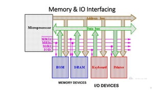
- 6. Memory & IO Interfacing 6 MEMORY DEVICES I/O DEVICES
- 7. ïš interface memory (RAM, ROM, EPROM'...) or I/O devices to 8086 microprocessor. Several memory chips or I/O devices can connected to a microprocessor. An address decoding circuit is used to select the required I/O device or a memory chip. 7
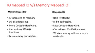
- 8. IO mapped IO V/s Memory Mapped IO Memory Mapped IO âĒ IO is treated as memory. âĒ 16-bit addressing. âĒ More Decoder Hardware. âĒ Can address 216=64k locations. âĒ Less memory is available. IO Mapped IO âĒ IO is treated IO. âĒ 8- bit addressing. âĒ Less Decoder Hardware. âĒ Can address 28=256 locations. âĒ Whole memory address space is available. 8
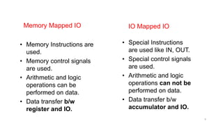
- 9. Memory Mapped IO âĒ Memory Instructions are used. âĒ Memory control signals are used. âĒ Arithmetic and logic operations can be performed on data. âĒ Data transfer b/w register and IO. IO Mapped IO âĒ Special Instructions are used like IN, OUT. âĒ Special control signals are used. âĒ Arithmetic and logic operations can not be performed on data. âĒ Data transfer b/w accumulator and IO. 9
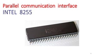
- 10. Parallel communication interface INTEL 8255 10
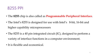
- 11. 8255 PPI âĒ The 8255 chip is also called as Programmable Peripheral Interface. âĒ The Intelâs 8255 is designed for use with Intelâs 8-bit, 16-bit and higher capability microprocessors âĒ The 8255 is a 40 pin integrated circuit (IC), designed to perform a variety of interface functions in a computer environment. âĒ It is flexible and economical. 11
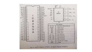
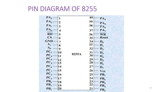
- 15. PIN DIAGRAM OF 8255 15
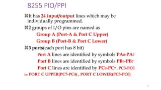
- 17. 8255 PIO/PPI ïšIt has 24 input/output lines which may be individually programmed. ïš2 groups of I/O pins are named as Group A (Port-A & Port C Upper) Group B (Port-B & Port C Lower) ïš3 ports(each port has 8 bit) Port A lines are identified by symbols PA0-PA7 Port B lines are identified by symbols PB0-PB7 Port C lines are identified by PC0-PC7 , PC3-PC0 ie: PORT C UPPER(PC7-PC4) , PORT C LOWER(PC3-PC0) 17
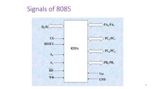
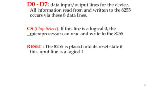
- 18. D0 - D7: data input/output lines for the device. All information read from and written to the 8255 occurs via these 8 data lines. CS (Chip Select). If this line is a logical 0, the microprocessor can read and write to the 8255. RESET : The 8255 is placed into its reset state if this input line is a logical 1 18
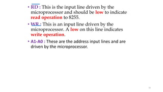
- 19. âĒ RD : This is the input line driven by the microprocessor and should be low to indicate read operation to 8255. âĒ WR : This is an input line driven by the microprocessor. A low on this line indicates write operation. âĒ A1-A0 : These are the address input lines and are driven by the microprocessor. 19
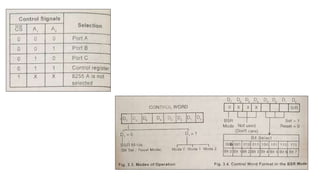
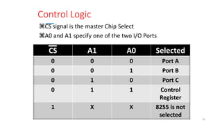
- 20. Control Logic ïšCS signal is the master Chip Select ïšA0 and A1 specify one of the two I/O Ports 20 CS A1 A0 Selected 0 0 0 Port A 0 0 1 Port B 0 1 0 Port C 0 1 1 Control Register 1 X X 8255 is not selected
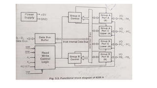
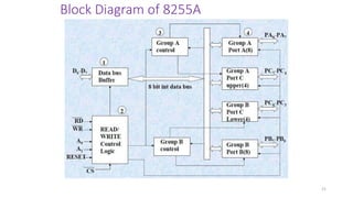
- 21. Block Diagram of 8255A 21
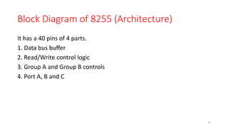
- 22. Block Diagram of 8255 (Architecture) It has a 40 pins of 4 parts. 1. Data bus buffer 2. Read/Write control logic 3. Group A and Group B controls 4. Port A, B and C 22
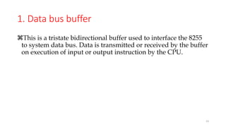
- 23. 1. Data bus buffer ïšThis is a tristate bidirectional buffer used to interface the 8255 to system data bus. Data is transmitted or received by the buffer on execution of input or output instruction by the CPU. 23
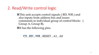
- 24. 2. Read/Write control logic ïšThis unit accepts control signals ( RD, WR ) and also inputs from address bus and issues commands to individual group of control blocks ( Group A, Group B). ïšIt has the following pins. CS , RD , WR , RESET , A1 , A0 24
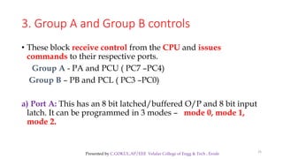
- 25. 3. Group A and Group B controls âĒ These block receive control from the CPU and issues commands to their respective ports. Group A - PA and PCU ( PC7 âPC4) Group B â PB and PCL ( PC3 âPC0) a) Port A: This has an 8 bit latched/buffered O/P and 8 bit input latch. It can be programmed in 3 modes â mode 0, mode 1, mode 2. 25 Presented by C.GOKUL,AP/EEE Velalar College of Engg & Tech , Erode
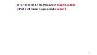
- 26. b) Port B: It can be programmed in mode 0, mode1 c) Port C : It can be programmed in mode 0 26
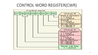
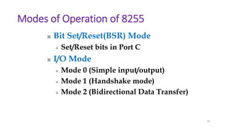
- 28. Modes of Operation of 8255 28 ïš Bit Set/Reset(BSR) Mode ïļ Set/Reset bits in Port C ïš I/O Mode ïļ Mode 0 (Simple input/output) ïļ Mode 1 (Handshake mode) ïļ Mode 2 (Bidirectional Data Transfer)
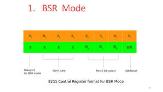
- 29. 1. BSR Mode 29
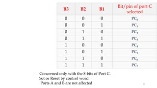
- 30. 30 B3 B2 B1 Bit/pin of port C selected 0 0 0 PC0 0 0 1 PC1 0 1 0 PC2 0 1 1 PC3 1 0 0 PC4 1 0 1 PC5 1 1 0 PC6 1 1 1 PC7 Concerned only with the 8-bits of Port C. Set or Reset by control word Ports A and B are not affected