This document discusses different design styles for integrated circuits including full-custom, standard cell, gate array, and FPGA. It compares the characteristics of each style such as cell size and placement, fabrication layers used, area, performance, design cost, and time-to-market. The document also discusses FPGA architecture, logic modules, switchboxes, segmentation models, and the physical design process of partitioning, placement, and routing for FPGAs. Multi-chip module and system-in-package designs are introduced along with the challenges of physical design automation for those domains.
1. The document discusses various topics in VLSI physical design automation including different design styles like FPGA, standard cell, and structured ASIC.
2. It compares the design styles based on factors like cell size, placement, routing, area, performance, and cost. FPGA is described as having fixed and programmable logic and interconnect resources.
3. The document also covers FPGA architecture including logic modules, routing resources, and I/O modules. It describes the physical design process of partitioning, placement, and routing for FPGAs which has different challenges compared to other design styles.
This document discusses digital VLSI design flows. It begins by acknowledging previous work that informed the presentation. It then discusses considerations in developing an electronic system, including components of the system. It describes integrated circuits based on application, fabrication technology, device, and device count. It discusses using standard or application-specific integrated circuits. It outlines a top-down design approach and terminology used in the design flow.
This document provides an introduction to VLSI design. It begins by defining VLSI as circuits containing over a million switching devices or logic gates. It then discusses the evolution of integrated circuits from SSI to VLSI and the trends in IC technology. The key advantages of MOS technology over BJT are summarized. The document outlines Moore's Law and provides evidence of its accuracy. It introduces the structured design methodology and top-down, bottom-up approaches. The various stages of the VLSI design flow and physical design cycle are described at a high level. Different design styles including full-custom, standard cell-based, and programmable logic are also summarized.
Implementation strategies for digital icsaroosa khan
油
The document discusses various digital integrated circuit design implementation strategies. It describes very large scale integration (VLSI) and the VLSI design cycle. It then covers Moore's law, productivity growth rates, and two main design implementation strategies - full custom circuit design and standard cell-based semi-custom design. The document provides details on standard cell libraries, floorplanning, gate arrays, and field programmable gate arrays (FPGAs), and concludes with a comparison of the different design styles.
VLSI design involves integrating millions of transistors onto a single chip. There are various design styles including full custom, standard cell, gate array, and FPGA. Full custom designs have fully customized cells and layouts but require more design time. Standard cell and gate array styles use predesigned cells, reducing design time but only customizing interconnect layers. FPGA designs have no custom masks and the fastest design turnaround time.
System on Chip is a an IC that integrates all the components of an electronic system. This presentation is based on the current trends and challenges in the IP based SOC design.
System on Chip (SoC) designs integrate multiple components, such as processors, memory, and I/O, onto a single chip. This consolidation provides benefits like reduced cost and power consumption compared to using multiple discrete chips. The SoC design process involves specifying system functionality, defining an architecture to implement it using reusable intellectual property cores, and employing techniques like hardware-software codesign and spiral development models to improve productivity. Key challenges in SoC design include managing complexity, meeting tight schedules, and ensuring high design quality and verification.
2017 Atlanta Regional User Seminar - Real-Time Microgrid DemosOPAL-RT TECHNOLOGIES
油
This document discusses challenges in simulating distributed energy resources and microgrids in real-time including bidirectional power flow, integration of new technologies, controls, islanding operations, and communication networks. It also describes a real-time hardware-in-the-loop simulation platform that models a microgrid test system containing generators, loads, energy storage and PV to evaluate commercial microgrid controllers under different operating conditions and grid connection scenarios.
The document discusses trends in integration technologies such as VLSI. It describes how VLSI has allowed for more compact, lower power, and higher speed integrated circuits. It classifies integrated circuits based on application, fabrication technique, technology, and device count. It then discusses the history of integrated circuits from the transistor in 1947 to modern chips containing tens of millions of transistors. It outlines drivers for VLSI technology including smaller sizes, lower power, and reduced costs.
Performance and Flexibility for Mmultiple-Processor SoC DesignYalagoud Patil
油
Concepts, limitations of traditional ASIC design
Extensible processors as an alternative to RTL
Toward multiple-processor SoCs
Processors and disruptive technology
Conclusions
This document outlines the course contents for a VLSI Design course. The course covers six units: (1) an introduction to VLSI design including Moore's Law and design challenges, (2) VLSI circuit design processes and technologies, (3) analysis of CMOS logic circuits, (4) advanced CMOS logic circuit techniques, (5) memories, and (6) testing and testability. The goal of the course is to provide students with knowledge of very large scale integration circuits, which are essential components in modern electronic devices.
Field Programmable Gate Arrays : ArchitectureUsha Mehta
油
This document discusses FPGA architecture and programming. It begins with an acknowledgement of sources used to create the presentation. It then discusses how FPGA programming differs from microprocessor programming. The document covers the evolution of FPGAs from CPLDs and their advantages over ASICs. It discusses the programmability of FPGAs in logic, interconnects, and input/output. Examples of Xilinx and Altera FPGA architectures are provided. Applications and advantages of FPGAs are also summarized.
This document provides an overview of Module 1 of the ECIE 4343 Very Large Scale Integrated Circuits (VLSI) Design course. The module introduces course logistics, content, and design implementation options. It outlines topics that will be covered including VLSI economy, MOSFET characteristics, circuit layout, fabrication, and CAD tools. A course schedule is provided listing weekly topics and assignments. Assessment breakdown consists of a final exam, project, midterm, and assignments/quizzes. Historical trends in transistor size reduction and integrated circuit scaling are reviewed.
This document provides an overview of digital CMOS logic circuits. It discusses CMOS technology and how it has become the dominant technology for digital circuit implementation due to its low power dissipation and high integration density. The document then covers different logic circuit families including CMOS, bipolar, BiCMOS, and GaAs. It discusses characteristics of logic circuits like noise margins, propagation delay, power dissipation, silicon area, and fan-in/fan-out. Different digital system design styles using off-the-shelf components or custom VLSI chips are presented. The role of design abstraction and computer aids in facilitating large digital system design is also covered. Finally, the document discusses CMOS inverter circuit operation and the voltage transfer
System on Chip (SoC) integrates processor, memory and other components onto a single chip. Advances in VLSI technology allow millions of transistors to be placed on a single die, enabling entire systems to be implemented as SoCs. This provides benefits like lower cost, power consumption and size compared to discrete components. However, designing highly complex SoCs presents challenges related to design time, verification and complexity. Reusing pre-designed and verified intellectual property (IP) cores is a solution that helps manage this complexity.
This document provides an overview of an ASIC/FPGA technology and design flow course. It discusses the course organization, material, schedule, and recommended literature. The course will cover FPGA and ASIC design flows, including Verilog, synthesis, simulation, and implementation. It will also discuss chip structures, technologies, applications and the semiconductor industry. Students will complete projects to design an FPGA peripheral and an ASIC, with design reviews to mimic industry practice. The goal is to prepare students for careers in chip design and verification.
This document provides an overview of the ASIC back-end design flow, including timing driven placement. It discusses the inputs to the Astro placement and routing tool, including the gate-level netlist, standard cell library, and timing constraints. It describes key aspects of the placement process, including floorplanning, placement rows, and timing driven placement to optimize critical paths. The goal is to meet all timing constraints by balancing timing, area, power, and signal integrity.
3D packaging stacks separate chips in a single package to save space without integrating the chips. Monolithic 3D ICs build components in layers on a single wafer then dice it, avoiding alignment and bonding issues. Multi-wafer 3D ICs build components on separate wafers, which must be aligned, bonded, and thinned with vertical connections added through silicon vias. 3D ICs promise benefits like reduced cost from improved yield, lower power from shorter wires, and new design possibilities from added connectivity, but challenges include heat dissipation, design complexity, and testing of independent dies.
FPGAs can implement an entire system on a single chip and offer reprogrammability after manufacturing through bitstream programming. They allow for faster design times compared to custom ICs due to lack of physical design steps. However, FPGAs are slower than custom ICs for complex designs and consume more power. The FPGA design flow involves HDL design entry, synthesis, implementation through place and route, and bitstream programming. FPGAs contain configurable logic blocks, I/O pads, interconnects, and switch boxes. Common FPGA technologies include SRAM, antifuse, and EEPROM/EPROM which offer different characteristics of volatility, reprogrammability and fabrication process. Popular FPGA families are
This document provides an overview of FPGA architecture. It discusses the available choices for digital designers between using discrete components or programmable logic devices. It then examines FPGA technology in more detail, including the interconnect framework, field programmability using different technologies like SRAM, antifuse, EPROM, and EEPROM. Commercially available FPGA devices from Xilinx and Altera are also summarized.
This document describes the ASIC design flow, including various design methodologies like full custom, standard cell, and gate array. It discusses the front-end design steps like specifications, design entry, functional verification, and synthesis. It also covers back-end steps like floorplanning, placement, routing, timing analysis, and GDS-II generation. Key techniques like design for test (DFT), scan insertion, and formal verification are also summarized. The document provides an overview of the complete digital ASIC design process.
The document provides an introduction to the method of logical effort, which can be used to estimate delay in CMOS circuits. The method uses a simple delay model to allow rapid comparison of different logic structures and help select the fastest design. It defines the concept of logical effort to characterize the delay properties of different logic gates independent of load and transistor size. Logical effort, along with electrical effort and parasitic delay, is used to formulate a delay equation for logic gates. Examples are provided to demonstrate calculating logical effort values for common gates.
This document discusses CMOS digital integrated circuits and combinational logic circuits. It covers static CMOS circuits, NMOS and PMOS transistors, threshold calculations for logic gates like NOR and NAND, layout of logic gates, and device sizing in complex gates. The key points are:
- Static CMOS circuits have a continuous low-resistance path between outputs and power/ground.
- Threshold calculations allow NOR and NAND gates to switch at VDD/2.
- Layout and stick diagrams show transistor positions and connections for logic gates.
- Device sizing methods ensure all signal paths can support switching.
This document outlines the steps to create a Vivado project, including setting the project name and location, selecting the project type as RTL, adding or creating source files and optional IP, selecting the target FPGA board parts, editing the project to create source files and define modules, and writing Verilog code and a test bench for simulation.
This document discusses content-addressable memories (CAMs), read-only memories (ROMs), and programmable logic arrays (PLAs). It begins by describing CAM cell design and operation, then covers ROM cell layout and decoding. Programmable ROMs like PROMs and EPROMs are also introduced. Finally, PLAs are discussed as a way to implement logic functions using NOR gates, along with an example implementation of a finite state machine for a robot ant using a PLA.
This document discusses the operation and modeling of MOSFET transistors. It begins by describing the basic structure and operation of an n-type MOSFET. It then provides some important equations that model the inversion layer charge and threshold voltage. The document goes on to discuss modeling the transistor behavior in different regimes, including gradual channel approximation, sub-threshold behavior, and saturation. It also compares MOSFETs to BJTs and discusses factors that affect transistor performance such as mobility and threshold voltage control.
This document discusses sequential circuits and their analysis and design. It begins by defining sequential circuits and their basic components like latches and flip-flops. It then covers analyzing synchronous sequential circuits using their output functions, state equations, and state tables. The document concludes by outlining the steps for designing a synchronous sequential circuit from its specification.
The Golden Gate Bridge a structural marvel inspired by mother nature.pptxAkankshaRawat75
油
The Golden Gate Bridge is a 6 lane suspension bridge spans the Golden Gate Strait, connecting the city of San Francisco to Marin County, California.
It provides a vital transportation link between the Pacific Ocean and the San Francisco Bay.
Air pollution is contamination of the indoor or outdoor environment by any ch...dhanashree78
油
Air pollution is contamination of the indoor or outdoor environment by any chemical, physical or biological agent that modifies the natural characteristics of the atmosphere.
Household combustion devices, motor vehicles, industrial facilities and forest fires are common sources of air pollution. Pollutants of major public health concern include particulate matter, carbon monoxide, ozone, nitrogen dioxide and sulfur dioxide. Outdoor and indoor air pollution cause respiratory and other diseases and are important sources of morbidity and mortality.
WHO data show that almost all of the global population (99%) breathe air that exceeds WHO guideline limits and contains high levels of pollutants, with low- and middle-income countries suffering from the highest exposures.
Air quality is closely linked to the earths climate and ecosystems globally. Many of the drivers of air pollution (i.e. combustion of fossil fuels) are also sources of greenhouse gas emissions. Policies to reduce air pollution, therefore, offer a win-win strategy for both climate and health, lowering the burden of disease attributable to air pollution, as well as contributing to the near- and long-term mitigation of climate change.
This presentation provides an in-depth analysis of structural quality control in the KRP 401600 section of the Copper Processing Plant-3 (MOF-3) in Uzbekistan. As a Structural QA/QC Inspector, I have identified critical welding defects, alignment issues, bolting problems, and joint fit-up concerns.
Key topics covered:
Common Structural Defects Welding porosity, misalignment, bolting errors, and more.
Root Cause Analysis Understanding why these defects occur.
Corrective & Preventive Actions Effective solutions to improve quality.
Team Responsibilities Roles of supervisors, welders, fitters, and QC inspectors.
Inspection & Quality Control Enhancements Advanced techniques for defect detection.
Applicable Standards: GOST, KMK, SNK Ensuring compliance with international quality benchmarks.
This presentation is a must-watch for:
QA/QC Inspectors, Structural Engineers, Welding Inspectors, and Project Managers in the construction & oil & gas industries.
Professionals looking to improve quality control processes in large-scale industrial projects.
Download & share your thoughts! Let's discuss best practices for enhancing structural integrity in industrial projects.
Categories:
Engineering
Construction
Quality Control
Welding Inspection
Project Management
Tags:
#QAQC #StructuralInspection #WeldingDefects #BoltingIssues #ConstructionQuality #Engineering #GOSTStandards #WeldingInspection #QualityControl #ProjectManagement #MOF3 #CopperProcessing #StructuralEngineering #NDT #OilAndGas
Preface: The ReGenX Generator innovation operates with a US Patented Frequency Dependent Load
Current Delay which delays the creation and storage of created Electromagnetic Field Energy around
the exterior of the generator coil. The result is the created and Time Delayed Electromagnetic Field
Energy performs any magnitude of Positive Electro-Mechanical Work at infinite efficiency on the
generator's Rotating Magnetic Field, increasing its Kinetic Energy and increasing the Kinetic Energy of
an EV or ICE Vehicle to any magnitude without requiring any Externally Supplied Input Energy. In
Electricity Generation applications the ReGenX Generator innovation now allows all electricity to be
generated at infinite efficiency requiring zero Input Energy, zero Input Energy Cost, while producing
zero Greenhouse Gas Emissions, zero Air Pollution and zero Nuclear Waste during the Electricity
Generation Phase. In Electric Motor operation the ReGen-X Quantum Motor now allows any
magnitude of Work to be performed with zero Electric Input Energy.
Demonstration Protocol: The demonstration protocol involves three prototypes;
1. Protytpe #1, demonstrates the ReGenX Generator's Load Current Time Delay when compared
to the instantaneous Load Current Sine Wave for a Conventional Generator Coil.
2. In the Conventional Faraday Generator operation the created Electromagnetic Field Energy
performs Negative Work at infinite efficiency and it reduces the Kinetic Energy of the system.
3. The Magnitude of the Negative Work / System Kinetic Energy Reduction (in Joules) is equal to
the Magnitude of the created Electromagnetic Field Energy (also in Joules).
4. When the Conventional Faraday Generator is placed On-Load, Negative Work is performed and
the speed of the system decreases according to Lenz's Law of Induction.
5. In order to maintain the System Speed and the Electric Power magnitude to the Loads,
additional Input Power must be supplied to the Prime Mover and additional Mechanical Input
Power must be supplied to the Generator's Drive Shaft.
6. For example, if 100 Watts of Electric Power is delivered to the Load by the Faraday Generator,
an additional >100 Watts of Mechanical Input Power must be supplied to the Generator's Drive
Shaft by the Prime Mover.
7. If 1 MW of Electric Power is delivered to the Load by the Faraday Generator, an additional >1
MW Watts of Mechanical Input Power must be supplied to the Generator's Drive Shaft by the
Prime Mover.
8. Generally speaking the ratio is 2 Watts of Mechanical Input Power to every 1 Watt of Electric
Output Power generated.
9. The increase in Drive Shaft Mechanical Input Power is provided by the Prime Mover and the
Input Energy Source which powers the Prime Mover.
10. In the Heins ReGenX Generator operation the created and Time Delayed Electromagnetic Field
Energy performs Positive Work at infinite efficiency and it increases the Kinetic Energy of the
system.
Indian Soil Classification System in Geotechnical EngineeringRajani Vyawahare
油
This PowerPoint presentation provides a comprehensive overview of the Indian Soil Classification System, widely used in geotechnical engineering for identifying and categorizing soils based on their properties. It covers essential aspects such as particle size distribution, sieve analysis, and Atterberg consistency limits, which play a crucial role in determining soil behavior for construction and foundation design. The presentation explains the classification of soil based on particle size, including gravel, sand, silt, and clay, and details the sieve analysis experiment used to determine grain size distribution. Additionally, it explores the Atterberg consistency limits, such as the liquid limit, plastic limit, and shrinkage limit, along with a plasticity chart to assess soil plasticity and its impact on engineering applications. Furthermore, it discusses the Indian Standard Soil Classification (IS 1498:1970) and its significance in construction, along with a comparison to the Unified Soil Classification System (USCS). With detailed explanations, graphs, charts, and practical applications, this presentation serves as a valuable resource for students, civil engineers, and researchers in the field of geotechnical engineering.
2. 2
3/3/2023
Other Design Styles: FPGA
Field Programmable Gate Array
First introduced by Xilinx in 1984.
Pre-fabricated devices and interconnect, which are
programmable by user.
Advantages:
short turnaround time.
low manufacturing cost.
fully testable.
re-programmable.
Particularly suitable for prototyping, low or medium-
volume production, device controllers, etc.
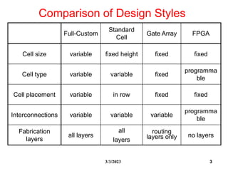
3. 3
3/3/2023
Comparison of Design Styles
Full-Custom
Standard
Cell
Gate Array FPGA
Cell size variable fixed height fixed fixed
Cell type variable variable fixed
programma
ble
Cell placement variable in row fixed fixed
Interconnections variable variable variable
programma
ble
Fabrication
layers
all layers
all
layers
routing
layers only no layers
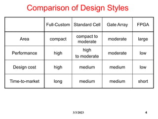
4. 4
3/3/2023
Comparison of Design Styles
Full-Custom Standard Cell Gate Array FPGA
Area compact
compact to
moderate
moderate large
Performance high
high
to moderate
moderate low
Design cost high medium medium low
Time-to-market long medium medium short
5. 5
3/3/2023
Programming Technologies
SRAM to control pass transistor / multiplexer
EPROM UV light Erasable PROM
EEPROM Electrically Erasable PROM
Antifuses One time programmable
They are different in ease of manufacturing,
manufacturing reliability, area, ON and OFF
resistance, parasitic capacitance, power consumption,
re-programmability.
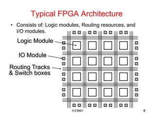
8. 8
3/3/2023
Two Types of Logic Modules
Look-Up Table (LUT) based:
A block of RAM to store the truth table.
A k-input 1-output functions needs 2k bits.
k is usually 5 or 6.
Multiplexer based: e.g., f=ABC+ABC
C
B
A
A
B
f
12. 12
3/3/2023
Comparison of Segmentation Models
The segmented model provides better utilization of
routing resources.
However, segmented model uses more fuses or
programmable switches.
The delay of a net is directly proportional to the # of
fuses or programmable switches in the route
Manhattan-distance based delay model does NOT work
anymore
The segmented model is slower in general
13. 13
3/3/2023
Physical Design of FPGAs
Very different from other design styles
Architecture dependent:
LUT or Multiplexer in logic modules
Type of switchboxes used
Type of segmentation model used
......
Physical Design:
Partitioning
Floorplanning/Placement
Routing
14. 14
3/3/2023
Partitioning
Want to partition the circuit such that each partition
(cluster) can be implemented by a logic module.
Also called Clustering.
# of I/O pins, not cluster sizes, is important.
(For multiplexer based logic modules, functionality of
clusters is also important.)
Example:
Using 4-LUTs
16. 16
3/3/2023
Routing
Global routing:
Similar to global routing in other design styles.
Minimize wire length and balance densities.
Detailed routing:
Very different from other design styles.
Different algorithms for different segmentation models.
Channels and switchboxes have fixed capacities.
17. 17
3/3/2023
Structured ASIC
New buzz word, but essentially gate array
Mask reconfigurable
Not field reconfigurable
Between FPGA and standard cells
Balance delay/performance and mask cost
Only programmable once
by vias (e.g., Via-Programmable Gate Array VPGA)
19. 19
3/3/2023
MCM and SiP
Multi-Chip Module
System in package (SiP)
Different package styles
Thermal consideration for 3D
Alternative packaging approach for high performance
systems.
Similar to PCB and IC layout problems, but
PCB layout tools cannot handle the dense and complex wiring
structure of MCM.
IC layout tools cannot handle the complex electrical, thermal
and geometrical constraints.
21. 21
3/3/2023
Partitioning
Partitioning a circuit so that each sub-circuit can be
implemented into a chip.
MCM may contain as many as 100 chips.
Need to consider timing constraints and thermal
constraints
In addition, also need to consider traditional I/O
constraints and area constraints.
22. 22
3/3/2023
Placement
# of components is much less as compared to IC
placement.
However, need to consider timing constraints and
thermal constraints (as bare chips are placed close to
each other).
Routing is done in routing layers, not between chips.
So no routing region needs to be allocated.
23. 23
3/3/2023
Routing
Main objective is to satisfy timing constraints.
Another objective is to minimize # of routing layers, not to
minimize routing area.
Cost is directly proportional to # of layers
Crosstalk, skin effect and parasitic effect are important
considerations.
Wires are of smaller pitch and more dense than PCB layout.
25. 25
3/3/2023
What Have Been Taught?
Introduced different problems in Physical Design.
Numerous algorithms which are different in terms of
design styles
objectives
constraints
techniques
optimality
efficiency
robustness
.....
26. 26
3/3/2023
What Is Important?
Understand the problems
How to formulate the problems, represent the constraints,
solutions, etc.
Reasonable assumptions/abstractions
Know fundamental algorithms to solve the problems.
However, the world keeps on changing:
technology
objectives
constraints
requirement on solution quality
computational power
It is more important to learn how to think
formulate the problem
solve it smartly
27. 27
3/3/2023
Problem Solving Techniques
Greedy Algorithm
Simulated Annealing/Genetic Algorithm
Mathematical Programming
Linear, Quadratic, Integer Linear, geometric, posynomial,
Dynamic Programming
Reduction to graph problems
min-cut, max-cut, shortest path, longest path, bipartite matching,
minimum spanning tree, etc.
Divide-and-Conquer
Many different heuristics
....
31. 31
3/3/2023
Technology Trend and Challenges
Source:
ITRS03
Interconnect determines the overall performance
In addition: noise, power => Design closure
Furthermore: manufacturability => Manufacturing closure
32. 32
3/3/2023
New Trends in Physical Design
For nanometer IC designs, interconnect dominates
New physical effects
Noise: coupling, P/G noise
Power: leakage, power/voltage islands
Manufacturability: yield, printability
Reliability,
More and more vertical integration
Logic synthesis coupled with physical design
Interconnect optimizations & design planning
Physical design as a bridge between lower level modeling and
higher level optimization/planning
Existing CAD algorithms are far away from optimal
33. 33
3/3/2023
Check points
Problem solving skills on underlying physical
design algorithms
Know whats behind the scene of CAD tools
Know the trend and critique ability if given a new
research paper
Project study of a topic of your choice and
implementation (through class project)
Presentation skill
Paper writing and job preparation