ARM CORTEX M3 PPT
132 likes37,020 views

This Presentation describes the ARM CORTEX M3 core processor with the details of the core peripherals. Soon a CORTEX base controller(STM32F100RBT6) ppt will be uploaded. For more information mail me at:gaurav.iitkg@gmail.com.


More Related Content
What's hot (20)
Similar to ARM CORTEX M3 PPT (20)


Recently uploaded (20)


ARM CORTEX M3 PPT
- 1. ARM CORTEX PROCESSOR Gaurav Verma A i P fAssistant Professor Department of Electronics and Communication Engineering Jaypee Institute of Information and TechnologyJ yp gy Sector-62, Noida, Uttar Pradesh, India. il @jii i ii k @ il 1 Email: gaurav.verma@jiit.ac.in, gaurav.iitkg@gmail.com
- 2. WHY CORTEX? G t f ffi i ll i k t b d ith tGreater performance efficiency: allowing more work to be done without increasing the frequency or power requirements. Low power consumption: enabling longer battery life, especially criticalLow power consumption: enabling longer battery life, especially critical in portable products including wireless networking applications. Enhanced determinism: guaranteeing that critical tasks and interruptsg g p are serviced as quickly as possible and in a known number of cycles. Ease of use: providing easier programmability and debugging for the b f b d b bgrowing number of 8-bit and 16-bit users migrating to 32 bits. Lower cost solutions: reducing 32-bit-based system costs close to those of legacy 8 bit and 16 bit devices and enabling low end 32 bitof legacy 8-bit and 16-bit devices and enabling low-end, 32-bit microcontrollers to be priced at less than US$1 for the first time. Wide choice of development tools: from low-cost or free compilers to 2 f p p full-featured development suites from many development tool vendors
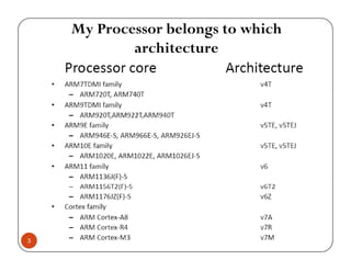
- 3. My Processor belongs to which architecturearchitecture 3
- 4. ARM Architecture road map 4
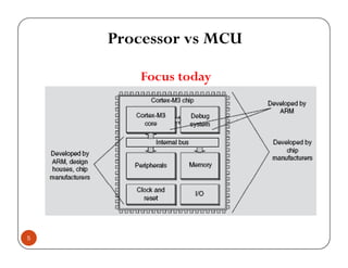
- 5. Processor vs MCU Focus todayy 5
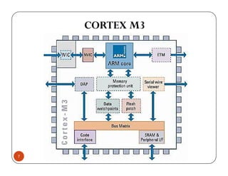
- 7. CORTEX M3 7
- 8. Features of ARM CORTEX M3 Processor Harvard bus architectureHarvard bus architecture –3-stage pipeline with branch speculation Configurable nested vectored interrupt controller (NVIC) Wake-up Interrupt Controller (WIC) –Enables ultra low-power standby operation Extended configurability of debug and trace capabilitiesg y g p –More flexibility for meeting specific market requirements Optional components for specific market reqs. M P t ti U it (MPU)–Memory Protection Unit (MPU) –EmbeddedTrace Macrocell™(ETM™) Support for fault robust implementations via configurable observation interface –EC61508 standard SIL3 certification Physical IP support 8 y pp –Power Management Kit™(PMK) + low-power standard cell libraries and memories enable0.18μm Ultra-Low Leakage (ULL) process
- 9. ARM Cortex Pipeline H d h S I D b blHarvard architecture- Separate Instruction & Data buses, enable parallel fetch & store, Advanced 3-Stage Pipeline Includes Branch Forwarding & Speculation,AdditionalWrite-Back via Bus Matrix.Forwarding & Speculation,AdditionalWrite Back via Bus Matrix. 9
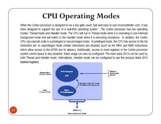
- 10. 10
- 11. CPU Registers • There are 16 registers, which are of 32 bit wide. • Register R0-R12 are general purpose registers. • Register R13 is used as the stack pointer• Register R13 is used as the stack pointer. • There are two stacks i.e. main stack and process stack depends upon in which mode the processor is working. • R14 is the link register, which is used to store the return address of procedure call. For nested calls the compiler will automatically store the R14 on the stack. • R15 is the normal program counter. 11
- 12. Program Status Register: XPSR 12
- 13. APSRAPSR 13
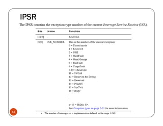
- 14. IPSR 14
- 15. EPSR 15
- 16. EPSR 16
- 18. 18
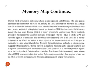
- 21. Memory Map 21
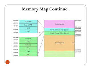
- 23. Memory Map Continue..y p 23
- 24. Unaligned Memory Accessg y 24
- 25. Bit Bandingg 25
- 26. 26
- 27. 27
- 28. 28
- 29. Accessing of Bit Band & Alias Regiong g 29
- 30. Read ModifyWriteVs Bit Bandingy g 30
- 31. SystemTimer (SysTick)Syste e (Sys c ) 31
- 32. SysTick Control & Status Registery g 32
- 33. SysTick ReloadValue Registery g 33
- 34. SysTick CurrentValue Register SysTick Usage 34
- 35. ARM7 vs ARM CORTEX INTERRUPTARM7 vs ARM CORTEX INTERRUPT HANDLING 35
- 36. Features Description of NVIC N d V d I C ll (NVIC) d h hNested Vectored Interrupt Controller (NVIC) integrated with the processor for low latency Configurable number 1 to 240 of external interrupts–Configurable number, 1 to 240, of external interrupts –Configurable number, 3 to 8, of bits of priority. –Dynamic reprioritization of interruptsDynamic reprioritization of interrupts. –Priority grouping. This allows selection of pre-empting interrupt levels and non pre-empting interrupt levelsp p p g p –Support for tail-chaining, and late arrival, of interrupts. This enables back-to-back interrupt processing without the overhead of state saving and restoration between interrupts –Processor state automatically saved on interrupt entry, and restored on interrupt exit with no instruction overhead 36 restored on interrupt exit, with no instruction overhead.
- 37. 37
- 38. NVIC Operation Exception Entry & Exitp p y 38
- 40. Tail Chaining 40
- 42. Late Arrival 42
- 43. NVIC Configuration & Use 43
- 44. NVIC Configuration & Use 44
- 45. 45
- 46. 46
- 47. System Handler Priority Register 1 47
- 48. System Handler Priority Register 2 System Handler Priority Register 3 48
- 50. Interrupt Set Enable Registers 50
- 51. Interrupt Clear Enable Registers 51
- 52. Interrupt Set Pending Registers 52
- 53. Interrupt Clear Pending Registers 53
- 54. Interrupt Active Bit Registers 54
- 57. Application Interrupt and Reset Control Register 57
- 58. 58
- 59. 59
- 62. Level Sensitive and Pulse Interrupts 62
- 63. Hardware & Software Control 63
- 64. Hardware & Software Control 64
- 65. Entering Low Power Modes 65
- 66. Entering Low Power Modes 66