


More Related Content
Similar to Basic Electronics (EC20201 course) presentation (IIT KGP) (20)
Recently uploaded (20)


Basic Electronics (EC20201 course) presentation (IIT KGP)
- 1. BASIC ELECTRONICS(EC21201) DR. SHYAMAL KUMAR DAS MANDAL ADVANCED TECHNOLOGY DEVELOPMENT CENTRE, IIT KHARAGPUR sdasmandal@cet.iitkgp.ac.in
- 2. ’üČ Classify electronic components as passive or active. ’üČ Draw the voltage-current characteristics of diode, BJT and MOSFET ’üČ Draw the circuit for half-wave and full-wave rectifiers. ’üČ Compute peak and rms voltages for half- and full-wave rectifiers with filters. ’üČ Find values of resistors to bias a transistor amplifier circuit using BJT and MOSFET. ’üČ Draw the small signal equivalent for amplifier circuits. ’üČ Compute the low- and high voltage levels in BJT and MOSFET switches. ’üČ Understand the characteristics of ideal and practical operational amplifiers, circuit design with them and their analysis. ’üČ Draw the circuit diagrams for different applications of op-amp. ’üČ Compute the transfer function for feedback amplifiers and test whether the circuit oscillates. Course outcome
- 3. Course Contents: As in Annexure-1 Marking Scheme: TA 20 marks MidSem Exam 30 marks EndSem Exam 50 marks Lecture Schedule: THURS(03:00-03:55) , THURS(04:00-04:55) , FRI(02:00-02:55) Tutorial: FRI(03:00-03:55) Venue: NR111
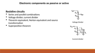
- 4. Electronic components as passive or active Resistive circuits ’é¦ Series and parallel combinations ’é¦ Voltage divider, current divider ’é¦ Thevenin equivalent, Norton equivalent and source transformation ’é¦ Superposition theorem Voltage Divider Current divider
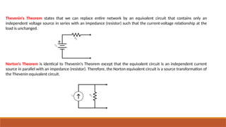
- 5. Thevenin's Theorem states that we can replace entire network by an equivalent circuit that contains only an independent voltage source in series with an impedance (resistor) such that the current-voltage relationship at the load is unchanged. Norton's Theorem is identical to Thevenin's Theorem except that the equivalent circuit is an independent current source in parallel with an impedance (resistor). Therefore, the Norton equivalent circuit is a source transformation of the Thevenin equivalent circuit.
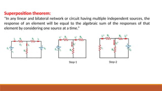
- 6. Superposition theorem: ŌĆ£In any linear and bilateral network or circuit having multiple independent sources, the response of an element will be equal to the algebraic sum of the responses of that element by considering one source at a time.ŌĆØ Step-1 Step-2
- 7. RC, LC and RLC circuit ’é¦ Frequency response ’é¦ Series and parallel combinations ’é¦ Phasor notation and concept of impedance, lagging and leading Integrator Differentiator
- 8. Concept of Electron Emission Electron emission is defined as the liberation of electrons from any surface of a substance. Types of Electron Emission ’é¦ Thermionic Emission ’é¦ Field emission ’é¦ Secondary emission ’é¦ Photo-electric emission Energy Band: The range of energies possessed by an electron in a solid is known as energy band. Valence Band: The range of energies (i.e. band) possessed by valence electrons is known as valence band. Conduction Band: The range of energies (i.e. band) possessed by conduction band electrons is known as conduction band. Forbidden energy gap: The separation between conduction band and valence band on the energy level diagram is known as forbidden energy gap.
- 9. Classification of material according to electrical conductivity (Conductor, Semiconductor & Insulator) Insulators. are those substances which do not allow the passage of electric current through them. In terms of energy band, the valence band is full while the conduction band is empty. Further, the energy gap between valence and conduction bands is very large (15 eV). Therefore, a very high electric field is required to push the valence electrons to the conduction band. However, when the temperature is raised, some of the valence electrons may acquire enough energy to cross over to the conduction band. Hence, the resistance of an insulator decreases with the increase in temperature i.e. an insulator has negative temperature coefficient of resistance. Conductors. are those substances which easily allow the passage of electric current through them. It is because there are a large number of free electrons available in a conductor. In terms of energy band, the valence and conduction bands overlap each other. Due to this overlapping, a slight potential difference across a conductor causes the free electrons to constitute electric current. Semiconductors. are those substances whose electrical conductivity lies in between conductors and insulators. In terms of energy band, the valence band is almost filled and conduction band is almost empty. Further, the energy gap between valence and conduction bands is very small. Therefore, comparatively smaller electric field(smaller than insulators but much greater than conductors) is required to push the electrons from the valence band to the conduction band. Forbidden energy gap 0.2-2.5eV
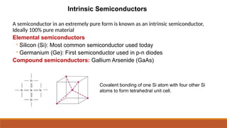
- 11. Intrinsic Semiconductors A semiconductor in an extremely pure form is known as an intrinsic semiconductor, Ideally 100% pure material Elemental semiconductors ŌŚ” Silicon (Si): Most common semiconductor used today ŌŚ” Germanium (Ge): First semiconductor used in p-n diodes Compound semiconductors: Gallium Arsenide (GaAs) Covalent bonding of one Si atom with four other Si atoms to form tetrahedral unit cell.
- 12. Effect of Temperature At 0K, Si is an insulator. As temperature increases, a bond can break, creating an electron and hole. Current can flow. kT E i g e BT n 2 2 3 ’ĆŁ ’ĆĮ B is a coefficient related to the specific semiconductor material
- 13. 1. Calculate the intrinsic carrier concentration in silicon at T = 300 K. 2. Calculate the intrinsic carrier concentration in gallium arsenide and germanium at T = 300 K.
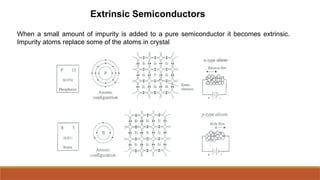
- 14. Extrinsic Semiconductors When a small amount of impurity is added to a pure semiconductor it becomes extrinsic. Impurity atoms replace some of the atoms in crystal
- 15. The doping process, which allows us to control the concentrations of free electrons and holes, determines the conductivity and currents in the material A fundamental relationship between the electron and hole concentrations in a semiconductor in thermal equilibrium is given by Carrier concentration If the donor concentration Nd is much larger than the intrinsic concentration Similarly, at room temperature, each acceptor atom accepts a valence electron, creating a hole. If the acceptor concentration Na is much larger than the intrinsic concentration
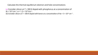
- 16. Calculate the thermal equilibrium electron and hole concentrations (a) Consider silicon at T = 300 K doped with phosphorus at a concentration of Nd = 1016 cm-3 . ni = 1.5 ├Ś 1010 cm-3 . (b) Consider silicon at T = 300 K doped with boron at a concentration of Na = 5 ├Ś 1016 cmŌłÆ3 .
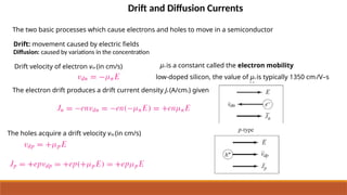
- 17. The two basic processes which cause electrons and holes to move in a semiconductor Drift and Diffusion Currents Drift: movement caused by electric fields Diffusion: caused by variations in the concentration Drift velocity of electron vdn (in cm/s) ╬╝n is a constant called the electron mobility low-doped silicon, the value of ╬╝n is typically 1350 cm2 /VŌĆōs The electron drift produces a drift current density Jn (A/cm2) given by The holes acquire a drift velocity vdp (in cm/s)
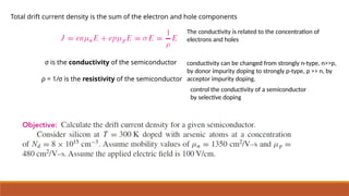
- 18. Total drift current density is the sum of the electron and hole components Žā is the conductivity of the semiconductor Žü = 1/Žā is the resistivity of the semiconductor conductivity can be changed from strongly n-type, n>>p, by donor impurity doping to strongly p-type, p >> n, by acceptor impurity doping. The conductivity is related to the concentration of electrons and holes control the conductivity of a semiconductor by selective doping
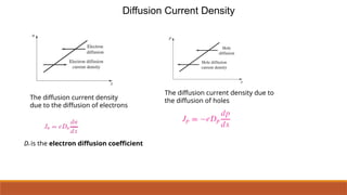
- 19. Diffusion Current Density The diffusion current density due to the diffusion of electrons Dn is the electron diffusion coefficient The diffusion current density due to the diffusion of holes
- 20. Calculate the diffusion current density for a given semiconductor
- 21. The mobility values in the drift current equations and the diffusion coefficient values in the diffusion current equations are not independent quantities. They are related by the Einstein relation, at room temperature Excess Carriers Non equilibrium electron and hole concentrations due to when a voltage is applied to, or a current exists in, a semiconductor device If the semiconductor is in a steady-state condition, the creation of excess electrons and holes will not cause the carrier concentration to increase indefinitely electronŌĆōhole recombination The mean time over which an excess electron and hole exist before recombination is called the excess carrier lifetime