Clock Skew 1
21 likes9,383 views
Clock skew refers to the difference in arrival times of a clock signal at different devices. Excessive clock skew can be minimized by buffering the clock signal so that all signals experience equal delays, adding delay to the data path to account for skew, reversing the clock signal direction to clock the destination register before the source, or using alternate phase clocking with two clock phases or opposite clock edges between sequential registers.
1 of 10


Recommended
Physical design-complete
Physical design-completeMurali Rai
Ėý
This document discusses various concepts related to physical design implementation. It describes the inputs and outputs of physical design tools, important checks to perform before starting design such as clock and high fanout net budgeting, and concepts like floorplanning, placement, routing, libraries, multi-voltage design, and clock tree synthesis and optimization.Clock Skew 2
Clock Skew 2rchovatiya
Ėý
Clock skew refers to differences in the arrival times of a clock signal at different flip-flops. Clock skew is caused by differences in delays along the paths from the clock generator to each flip-flop due to factors like wire lengths, gates, and clock edge inversion. The amount of clock skew affects calculations for the maximum clock frequency and allowable clock skew depends on the minimum setup and hold times of the flip-flops.Implementing Useful Clock Skew Using Skew Groups
Implementing Useful Clock Skew Using Skew GroupsM Mei
Ėý
Implementing useful skew through skew groups or manual buffer insertion can improve timing in a large memory block design. Skew groups define a target skew value for groups of clock pins before clock tree synthesis, resulting in a smaller clock tree, lower power increase, and less routing complexity compared to manual buffer insertion. Manual insertion precisely controls skew by adding buffers but dramatically increases clock cell count and power consumption versus skew groups. Both methods effectively improved setup timing for the memory block design.Divide by N clock
Divide by N clockMantra VLSI
Ėý
this presentation is based to construct different frequency divide by clock with reference to the system clock.VLSI-Physical Design- Tool Terminalogy
VLSI-Physical Design- Tool TerminalogyMurali Rai
Ėý
The physical design flow begins with placement which involves assigning exact locations to modules like gates and standard cells to minimize area and interconnect cost while meeting timing constraints, with the goal of enabling easier routing; placement tools take as input the netlist, floorplan, libraries, and constraints to perform global and detailed placement as well as optimization. The quality of placement significantly impacts the ability to route the design successfully.Eco
EcoRajesh M
Ėý
This document discusses engineering change orders (ECOs) used to fix timing, functional, power, and clock issues after physical design and sign-off. It describes the motivation for ECOs due to tool limitations and differences between implementation and sign-off. Common ECO techniques are listed for timing (driver upsizing, buffer insertion, etc.), power (vt-swapping, downsizing, etc.), and metal-only ECOs. Timing ECO tools from Synopsys, Cadence, and other vendors are also mentioned. Upcoming ECO technologies like dynamic power optimization and automatic legalization are noted.Multi mode multi corner (mmmc)
Multi mode multi corner (mmmc)shaik sharief
Ėý
This document discusses multi mode multi corner (MMMC) analysis for chip design. It defines that a mode is a set of design parameters like clocks and timing constraints, and a corner captures process, voltage, and temperature variations. It provides examples of multiple modes like normal, sleep, and test modes and corners for temperature, voltage, process variations, and parasitic interconnects. The document gives an example of analyzing a chip with 4 modes under 3 process-voltage-temperature corners and 3 parasitic interconnect corners, showing 9 analysis cases.ATPG Methods and Algorithms
ATPG Methods and AlgorithmsDeiptii Das
Ėý
The document discusses various ATPG (Automatic Test Pattern Generation) methods and algorithms. It provides an introduction to ATPG, explaining that ATPG generates test patterns to detect faults in circuits. It then covers major ATPG classifications like pseudorandom, ad-hoc, and algorithmic. Several algorithmic ATPG methods are described, including the D-algorithm, PODEM, FAN, and genetic algorithms. Sequential ATPG is more complex due to memory elements. The summary reiterates that testing large circuits is difficult and many ATPG methods have been developed for combinational and sequential circuits.Synopsys Fusion Compiler-Comprehensive RTL-to-GDSII Implementation System
Synopsys Fusion Compiler-Comprehensive RTL-to-GDSII Implementation SystemMostafa Khamis
Ėý
Fusion Compiler is the next-generation RTL-to-GDSII implementation system architected to address the complexities of advanced node designs and deliver up to 20% improved PPA while reducing Time To Results (TTR) by 2X. 2Overview of Primetime.pptx
2Overview of Primetime.pptxShivangPanara
Ėý
The document provides an overview of the PrimeTime static timing analysis tool. It describes PrimeTime's capabilities for design checks and analysis, how it fits into the Synopsys implementation flow, its compatibility with other Synopsys tools, and an overview of static timing analysis concepts like timing paths. The document also discusses starting a PrimeTime session, generating input files, and important commands and reports in PrimeTime like report_timing, report_qor, and analysis_coverage_report.Intellectual property in vlsi
Intellectual property in vlsiSaransh Choudhary
Ėý
Intellectual property (IP) in VLSI design refers to reusable logic or functionality units that can be licensed and used as building blocks in chip designs. There are two main types of IP: hard IP, which includes a pre-designed layout, and soft IP, which is delivered as synthesizable code. Soft IP is more vulnerable to theft since it is in a synthesizable form. Memories are often delivered as hard IP since they require careful analog design and peripheral circuitry to be useful. IP differs from custom chip design in that it is created before a specific use, with the goal of reuse across multiple designs. The IP lifecycle involves initial creation through specification, design, testing, and documentation, followed by integration intoSta by usha_mehta
Sta by usha_mehtaUsha Mehta
Ėý
This presentation is expert talk at Two day's International Webinar on "Testing and Verification of VLSI Design"13 static timing_analysis_4_set_up_and_hold_time_violation_remedy
13 static timing_analysis_4_set_up_and_hold_time_violation_remedyUsha Mehta
Ėý
The document discusses static timing analysis concepts including set-up time, hold time, timing violations, and techniques for fixing violations. It provides examples of how delays are considered in an ideal case without set-up/hold times versus cases with set-up/hold times. Methods for calculating maximum clock frequency and identifying violations are described. Ways to address violations including adjusting buffering, cell sizing, and placement are outlined. The role of static timing analysis in ASIC design flows is also summarized.STA vs DTA.pptx
STA vs DTA.pptxPayal Dwivedi
Ėý
This document discusses two types of timing analysis for integrated circuits (ICs): dynamic timing analysis (DTA) and static timing analysis (STA). DTA requires input stimuli to check both timing and functionality but is limited to small designs. STA is non-vector based, checks timing without input stimuli, and is suitable for large designs, though results may be pessimistic. While DTA only analyzes activated paths, STA considers all paths, potentially reporting false violations requiring exceptions.design-compiler.pdf
design-compiler.pdfFrangoCamila
Ėý
Synthesis & gate-level simulation is introduced. The key topics covered include basic concepts of logic synthesis using Design Compiler, including logic level optimization, mapping, boundary optimization, and static timing analysis. Simulation of the gate-level netlist generated after synthesis is also discussed. An example lab is outlined to synthesize a simple 8-bit microprocessor and simulate the gate-level netlist.fpga programming
fpga programmingAnish Gupta
Ėý
This document discusses the programming technologies and interconnect architectures used in different FPGA devices. It covers antifuse-based OTP technologies used in Actel FPGAs, SRAM-based reprogrammable technologies used in Xilinx FPGAs, and EPROM/EEPROM technologies used in Altera CPLDs. It also describes the segmented channel routing interconnect architecture used in Actel FPGAs and the LCA architecture used in Xilinx FPGAs.crosstalk minimisation using vlsi
crosstalk minimisation using vlsisubhradeep mitra
Ėý
This document summarizes techniques for minimizing crosstalk in VLSI designs. It discusses the VLSI design cycle and physical design cycle. Routing is a key stage that involves global and detailed routing. Crosstalk occurs due to mutual inductance and capacitance between wires and can affect signal integrity, delay, and timing. Basic approaches to reduce crosstalk include segregating wires, increasing spacing between wires, using ground shields, optimizing the net ordering and layer assignments. Specific techniques mentioned are widening spacing, minimizing wire heights and lengths of parallel runs, using differential routing, and routing orthogonal layers.14 static timing_analysis_5_clock_domain_crossing
14 static timing_analysis_5_clock_domain_crossingUsha Mehta
Ėý
This document discusses clock domain crossing (CDC) in integrated circuits with multiple clock domains. It defines CDC as transferring a signal between two asynchronous clock domains. Issues that can occur during CDC include metastability, data loss, and data incoherency. The document describes various synchronization techniques used to address these issues, including multi-flop synchronizers, gray coding, MUX recirculation synchronizers, and handshaking. It emphasizes that simulation and timing analysis alone are not sufficient to guarantee correct CDC behavior.Physical design 
Physical design Manjunath hosmani
Ėý
Physical design involves taking a synthesized netlist as input and performing floorplanning, placement, and routing to produce a physical layout. Key inputs include the netlist, timing constraints, physical libraries, and technology files. The process involves floor planning to determine block placement and routing areas, power planning to create the power distribution network, and pre-routing of standard cells and power grids. The goal is to meet timing constraints while minimizing area.Low Power Techniques
Low Power Techniqueskeshava murali
Ėý
This document discusses various low power techniques for integrated circuits. It begins by describing the increasing challenges of power consumption as device densities and clock frequencies increase while supply voltages and threshold voltages decrease. It then discusses different types of power consumption, including dynamic power, static power, leakage power from different sources, and how they can be reduced. The document covers many low power design techniques like multi-threshold CMOS, clock gating, multi-voltage, DVFS, and more. It discusses the evolution of these techniques and challenges in their implementation like timing issues, level shifters, and floorplanning for multi-voltage designs.Low power in vlsi with upf basics part 1
Low power in vlsi with upf basics part 1SUNODH GARLAPATI
Ėý
The document discusses low power design techniques in VLSI. It begins by explaining why low power has become important, especially with the rise of mobile devices. It then discusses the different sources of power consumption, including dynamic and static power. Several low power design techniques are covered, such as clock gating, multi-Vt libraries, multi-voltage design, and power gating. The document emphasizes analyzing power at the system level and using EDA tools to implement low power techniques throughout the design flow. Overall, it provides an overview of analyzing power consumption and the goals and methods of low power VLSI design.ASIC Design Flow | Physical Design | VLSI 
ASIC Design Flow | Physical Design | VLSI Jayant Suthar
Ėý
This document provides an overview of the ASIC design process, which includes the following main steps:
1. Front-end design including market research, specification, architecture, and RTL design.
2. Verification of the RTL code by verification engineers.
3. Synthesis of the RTL code into a gate-level netlist, followed by equivalence checking.
4. Physical design including placement and routing of standard cells, followed by extraction of parasitic components and timing analysis.
5. Physical verification including design rule checking and layout vs schematic checking.Basic synthesis flow and commands in digital VLSI
Basic synthesis flow and commands in digital VLSISurya Raj
Ėý
This document discusses logic synthesis, including the basic synthesis flow and commands, synthesis script flow, technology libraries, design objects like cells and ports, timing paths, and constraints like defining clocks and input/output delays. It provides examples of setting library variables, reading and writing designs, and applying constraints to clocks and I/O. The document contains information on synthesis tools and processes at a high level.Physical design 
Physical design Mantra VLSI
Ėý
VLSI Physical Design
Data preparation, import design, floorplan
Power planing
power ring, core power, IO power ring, pad, bump creattion.
Physical Verification.Low power in vlsi with upf basics part 2
Low power in vlsi with upf basics part 2SUNODH GARLAPATI
Ėý
The document discusses the Unified Power Format (UPF) standard for defining power intent and managing low power design verification. It provides an overview of UPF and describes some key UPF commands for defining power domains, supply ports and nets, power switches, power state tables, and level shifter strategies. The UPF standard allows specifying power intent separately from the design itself using the Tool Command Language (TCL) and helps enable power-aware simulation, synthesis and other tools in the design flow.Vlsi physical design
Vlsi physical designI World Tech
Ėý
The document discusses the physical design process for VLSI circuits. It describes the main steps as partitioning, floor planning and placement, routing, layout optimization, and extraction and verification. The goals of physical design are to minimize signal delays, interconnection area, and power usage. Physical design transforms the logical structure of a circuit into its physical layout.Advanced Low Power Techniques in Chip Design
Advanced Low Power Techniques in Chip DesignDr. Shivananda Koteshwar
Ėý
The document discusses techniques for reducing power consumption in integrated circuits and systems. It covers optimization opportunities at various levels of design from system to transistor level. Key techniques discussed include multi-voltage/multi-threshold designs, clock gating, power gating, dynamic voltage and frequency scaling, and reducing switching activity through logic restructuring. The document emphasizes that low power design requires a holistic approach across all levels of the design hierarchy.Understanding cts log_messages
Understanding cts log_messagesMujahid Mohammed
Ėý
Clock tree synthesis log messages provide information about:
1) Preprocessing steps like design updates, buffer characterization, and clock tree constraints.
2) The clock tree synthesis process which includes clustering, meeting timing targets, and reporting results.
3) Post processing steps like embedded clock tree optimization, DRC fixing, and placement legalization.Clock distribution in high speed board
Clock distribution in high speed boardPankaj Khodifad
Ėý
This document discusses clock distribution in high speed boards. It examines clock drivers, special clock routing rules, and circuits used to improve clock signal distribution. Precise clock distribution is important for correct system operation, as the clock provides the temporal frame of reference. Timing margin measures excess time in each clock cycle and protects against signal issues. Clock skew, or differences in clock arrival times, impacts timing margin and overall operating speed. Special techniques like low-impedance drivers, clock trees, and source termination of multiple lines can help optimize clock distribution.Types of cro
Types of croAnilAgarwal84
Ėý
The document discusses different types of oscilloscopes including dual trace CROs, dual beam CROs, digital storage oscilloscopes, and sampling oscilloscopes. A dual trace CRO uses a single electron beam but an electronic switch to display two input signals simultaneously. A dual beam CRO has two separate electron beams and deflection systems allowing two signals to be displayed together in real-time. Digital storage oscilloscopes digitize and store input signals, allowing slow signals to be analyzed. Sampling oscilloscopes take samples from input signals over multiple cycles to display high-frequency signals beyond the bandwidth of its amplifiers.More Related Content
What's hot (20)
Synopsys Fusion Compiler-Comprehensive RTL-to-GDSII Implementation System
Synopsys Fusion Compiler-Comprehensive RTL-to-GDSII Implementation SystemMostafa Khamis
Ėý
Fusion Compiler is the next-generation RTL-to-GDSII implementation system architected to address the complexities of advanced node designs and deliver up to 20% improved PPA while reducing Time To Results (TTR) by 2X. 2Overview of Primetime.pptx
2Overview of Primetime.pptxShivangPanara
Ėý
The document provides an overview of the PrimeTime static timing analysis tool. It describes PrimeTime's capabilities for design checks and analysis, how it fits into the Synopsys implementation flow, its compatibility with other Synopsys tools, and an overview of static timing analysis concepts like timing paths. The document also discusses starting a PrimeTime session, generating input files, and important commands and reports in PrimeTime like report_timing, report_qor, and analysis_coverage_report.Intellectual property in vlsi
Intellectual property in vlsiSaransh Choudhary
Ėý
Intellectual property (IP) in VLSI design refers to reusable logic or functionality units that can be licensed and used as building blocks in chip designs. There are two main types of IP: hard IP, which includes a pre-designed layout, and soft IP, which is delivered as synthesizable code. Soft IP is more vulnerable to theft since it is in a synthesizable form. Memories are often delivered as hard IP since they require careful analog design and peripheral circuitry to be useful. IP differs from custom chip design in that it is created before a specific use, with the goal of reuse across multiple designs. The IP lifecycle involves initial creation through specification, design, testing, and documentation, followed by integration intoSta by usha_mehta
Sta by usha_mehtaUsha Mehta
Ėý
This presentation is expert talk at Two day's International Webinar on "Testing and Verification of VLSI Design"13 static timing_analysis_4_set_up_and_hold_time_violation_remedy
13 static timing_analysis_4_set_up_and_hold_time_violation_remedyUsha Mehta
Ėý
The document discusses static timing analysis concepts including set-up time, hold time, timing violations, and techniques for fixing violations. It provides examples of how delays are considered in an ideal case without set-up/hold times versus cases with set-up/hold times. Methods for calculating maximum clock frequency and identifying violations are described. Ways to address violations including adjusting buffering, cell sizing, and placement are outlined. The role of static timing analysis in ASIC design flows is also summarized.STA vs DTA.pptx
STA vs DTA.pptxPayal Dwivedi
Ėý
This document discusses two types of timing analysis for integrated circuits (ICs): dynamic timing analysis (DTA) and static timing analysis (STA). DTA requires input stimuli to check both timing and functionality but is limited to small designs. STA is non-vector based, checks timing without input stimuli, and is suitable for large designs, though results may be pessimistic. While DTA only analyzes activated paths, STA considers all paths, potentially reporting false violations requiring exceptions.design-compiler.pdf
design-compiler.pdfFrangoCamila
Ėý
Synthesis & gate-level simulation is introduced. The key topics covered include basic concepts of logic synthesis using Design Compiler, including logic level optimization, mapping, boundary optimization, and static timing analysis. Simulation of the gate-level netlist generated after synthesis is also discussed. An example lab is outlined to synthesize a simple 8-bit microprocessor and simulate the gate-level netlist.fpga programming
fpga programmingAnish Gupta
Ėý
This document discusses the programming technologies and interconnect architectures used in different FPGA devices. It covers antifuse-based OTP technologies used in Actel FPGAs, SRAM-based reprogrammable technologies used in Xilinx FPGAs, and EPROM/EEPROM technologies used in Altera CPLDs. It also describes the segmented channel routing interconnect architecture used in Actel FPGAs and the LCA architecture used in Xilinx FPGAs.crosstalk minimisation using vlsi
crosstalk minimisation using vlsisubhradeep mitra
Ėý
This document summarizes techniques for minimizing crosstalk in VLSI designs. It discusses the VLSI design cycle and physical design cycle. Routing is a key stage that involves global and detailed routing. Crosstalk occurs due to mutual inductance and capacitance between wires and can affect signal integrity, delay, and timing. Basic approaches to reduce crosstalk include segregating wires, increasing spacing between wires, using ground shields, optimizing the net ordering and layer assignments. Specific techniques mentioned are widening spacing, minimizing wire heights and lengths of parallel runs, using differential routing, and routing orthogonal layers.14 static timing_analysis_5_clock_domain_crossing
14 static timing_analysis_5_clock_domain_crossingUsha Mehta
Ėý
This document discusses clock domain crossing (CDC) in integrated circuits with multiple clock domains. It defines CDC as transferring a signal between two asynchronous clock domains. Issues that can occur during CDC include metastability, data loss, and data incoherency. The document describes various synchronization techniques used to address these issues, including multi-flop synchronizers, gray coding, MUX recirculation synchronizers, and handshaking. It emphasizes that simulation and timing analysis alone are not sufficient to guarantee correct CDC behavior.Physical design
Physical design Manjunath hosmani
Ėý
Physical design involves taking a synthesized netlist as input and performing floorplanning, placement, and routing to produce a physical layout. Key inputs include the netlist, timing constraints, physical libraries, and technology files. The process involves floor planning to determine block placement and routing areas, power planning to create the power distribution network, and pre-routing of standard cells and power grids. The goal is to meet timing constraints while minimizing area.Low Power Techniques
Low Power Techniqueskeshava murali
Ėý
This document discusses various low power techniques for integrated circuits. It begins by describing the increasing challenges of power consumption as device densities and clock frequencies increase while supply voltages and threshold voltages decrease. It then discusses different types of power consumption, including dynamic power, static power, leakage power from different sources, and how they can be reduced. The document covers many low power design techniques like multi-threshold CMOS, clock gating, multi-voltage, DVFS, and more. It discusses the evolution of these techniques and challenges in their implementation like timing issues, level shifters, and floorplanning for multi-voltage designs.Low power in vlsi with upf basics part 1
Low power in vlsi with upf basics part 1SUNODH GARLAPATI
Ėý
The document discusses low power design techniques in VLSI. It begins by explaining why low power has become important, especially with the rise of mobile devices. It then discusses the different sources of power consumption, including dynamic and static power. Several low power design techniques are covered, such as clock gating, multi-Vt libraries, multi-voltage design, and power gating. The document emphasizes analyzing power at the system level and using EDA tools to implement low power techniques throughout the design flow. Overall, it provides an overview of analyzing power consumption and the goals and methods of low power VLSI design.ASIC Design Flow | Physical Design | VLSI
ASIC Design Flow | Physical Design | VLSI Jayant Suthar
Ėý
This document provides an overview of the ASIC design process, which includes the following main steps:
1. Front-end design including market research, specification, architecture, and RTL design.
2. Verification of the RTL code by verification engineers.
3. Synthesis of the RTL code into a gate-level netlist, followed by equivalence checking.
4. Physical design including placement and routing of standard cells, followed by extraction of parasitic components and timing analysis.
5. Physical verification including design rule checking and layout vs schematic checking.Basic synthesis flow and commands in digital VLSI
Basic synthesis flow and commands in digital VLSISurya Raj
Ėý
This document discusses logic synthesis, including the basic synthesis flow and commands, synthesis script flow, technology libraries, design objects like cells and ports, timing paths, and constraints like defining clocks and input/output delays. It provides examples of setting library variables, reading and writing designs, and applying constraints to clocks and I/O. The document contains information on synthesis tools and processes at a high level.Physical design
Physical design Mantra VLSI
Ėý
VLSI Physical Design
Data preparation, import design, floorplan
Power planing
power ring, core power, IO power ring, pad, bump creattion.
Physical Verification.Low power in vlsi with upf basics part 2
Low power in vlsi with upf basics part 2SUNODH GARLAPATI
Ėý
The document discusses the Unified Power Format (UPF) standard for defining power intent and managing low power design verification. It provides an overview of UPF and describes some key UPF commands for defining power domains, supply ports and nets, power switches, power state tables, and level shifter strategies. The UPF standard allows specifying power intent separately from the design itself using the Tool Command Language (TCL) and helps enable power-aware simulation, synthesis and other tools in the design flow.Vlsi physical design
Vlsi physical designI World Tech
Ėý
The document discusses the physical design process for VLSI circuits. It describes the main steps as partitioning, floor planning and placement, routing, layout optimization, and extraction and verification. The goals of physical design are to minimize signal delays, interconnection area, and power usage. Physical design transforms the logical structure of a circuit into its physical layout.Advanced Low Power Techniques in Chip Design
Advanced Low Power Techniques in Chip DesignDr. Shivananda Koteshwar
Ėý
The document discusses techniques for reducing power consumption in integrated circuits and systems. It covers optimization opportunities at various levels of design from system to transistor level. Key techniques discussed include multi-voltage/multi-threshold designs, clock gating, power gating, dynamic voltage and frequency scaling, and reducing switching activity through logic restructuring. The document emphasizes that low power design requires a holistic approach across all levels of the design hierarchy.Understanding cts log_messages
Understanding cts log_messagesMujahid Mohammed
Ėý
Clock tree synthesis log messages provide information about:
1) Preprocessing steps like design updates, buffer characterization, and clock tree constraints.
2) The clock tree synthesis process which includes clustering, meeting timing targets, and reporting results.
3) Post processing steps like embedded clock tree optimization, DRC fixing, and placement legalization.Similar to Clock Skew 1 (20)
Clock distribution in high speed board
Clock distribution in high speed boardPankaj Khodifad
Ėý
This document discusses clock distribution in high speed boards. It examines clock drivers, special clock routing rules, and circuits used to improve clock signal distribution. Precise clock distribution is important for correct system operation, as the clock provides the temporal frame of reference. Timing margin measures excess time in each clock cycle and protects against signal issues. Clock skew, or differences in clock arrival times, impacts timing margin and overall operating speed. Special techniques like low-impedance drivers, clock trees, and source termination of multiple lines can help optimize clock distribution.Types of cro
Types of croAnilAgarwal84
Ėý
The document discusses different types of oscilloscopes including dual trace CROs, dual beam CROs, digital storage oscilloscopes, and sampling oscilloscopes. A dual trace CRO uses a single electron beam but an electronic switch to display two input signals simultaneously. A dual beam CRO has two separate electron beams and deflection systems allowing two signals to be displayed together in real-time. Digital storage oscilloscopes digitize and store input signals, allowing slow signals to be analyzed. Sampling oscilloscopes take samples from input signals over multiple cycles to display high-frequency signals beyond the bandwidth of its amplifiers.VLSI Static Timing Analysis Intro Part 1
VLSI Static Timing Analysis Intro Part 1Amr Adel
Ėý
Part 1 of VLSI STA Documents
Topics Included:
- PPA Metrics
- Interconnect/Cell propagation delay
- Transition time
- Standard cells libraries
- Timing path calculations
- MTCMOS
- Setup / Hold / Tcq times
DESIGN AND IMPLEMENTATION OF AREA AND POWER OPTIMISED NOVEL SCANFLOP
DESIGN AND IMPLEMENTATION OF AREA AND POWER OPTIMISED NOVEL SCANFLOPVLSICS Design
Ėý
The power consumption of IC during test mode is higher than its normal mode. This brings the power as one of the major design constraints for todayâs low power design technologies. In normal scan based test circuits most of the power consumed due to the switching activity of scanflops during shift and capture cycles. In this paper a novel scanflop is presented which reduces the switching activity of the scanflop for clock and it reduces the power consumption of the circuit and it also reduces area and test time too. The proposed Dual Mode One Latch Double Edge Triggered (DMOL-DET) scanflop which shift the two bits of test vector in a clock cycle, during its test mode and captures the single data in a clock cycle during its data mode. The design and functionality of the proposed scanflop is discussed and compared with the different flipflops which shows that the proposed scan flop reduces the test time and clock switching activity by 50%, area by 30% and static power by 25%. A 20 gbs injection locked clock and data recovery circuit
A 20 gbs injection locked clock and data recovery circuitVLSICS Design
Ėý
This paper presents a 20 Gb/s injection-locked clock and data recovery (CDR) circuit for burst mode
applications. Utilizing a half rate injection-locked oscillator (ILO) in the proposed CDR circuit leads to
higher speed operation and lower power consumption. In addition, to accommodate process, voltage, and
temperature (PVT) variations and to increase the lock range, a frequency locked loop is proposed to use in
this circuit. The circuit is designed in 0.18 Ξm CMOS and the simulations for 27-1 pseudo random bit
sequence (PRBS) show that the circuit consumes 55.3 mW at 20 Gb/s, while the recovered clock rms jitter
is 1.1 psSta
StaPankaj Pandey
Ėý
This document discusses timing issues in flip-flops and synchronization circuits. It defines setup time and hold time, which are intervals before and after the clock edge when input data must remain stable. Metastability occurs when there are setup or hold time violations, causing the output to be unpredictable for some time before resolving to a stable value. To prevent metastability, techniques like adding synchronization stages or using flip-flops with higher mean time between failures can be used. Glitches in the clock signal can also cause metastability if they are detected as extra clock edges.Timing issues in digital circuits
Timing issues in digital circuitsaroosa khan
Ėý
The document discusses timing issues in digital circuits such as synchronization, clock skew, and clock jitter. It provides definitions and examples of these timing phenomena. Sources of skew and jitter are explained, including clock signal generation, manufacturing variations, interconnect variations, and environmental factors. The dynamic behavior of a CMOS inverter is analyzed by examining its parasitic capacitances. Solutions to timing issues include reducing clock skew through careful clock distribution, tolerating skew with circuit designs, and minimizing jitter.A 20 Gb/s INJECTION-LOCKED CLOCK AND DATA RECOVERY CIRCUIT
A 20 Gb/s INJECTION-LOCKED CLOCK AND DATA RECOVERY CIRCUITVLSICS Design
Ėý
This paper presents a 20 Gb/s injection-locked clock and data recovery (CDR) circuit for burst mode applications. Utilizing a half rate injection-locked oscillator (ILO) in the proposed CDR circuit leads to higher speed operation and lower power consumption. In addition, to accommodate process, voltage, and temperature (PVT) variations and to increase the lock range, a frequency locked loop is proposed to use in this circuit. The circuit is designed in 0.18 Âĩm CMOS and the simulations for 27-1 pseudo random bit sequence (PRBS) show that the circuit consumes 55.3 mW at 20 Gb/s, while the recovered clock rms jitter is 1.1 ps.
A 20 Gb/s INJECTION-LOCKED CLOCK AND DATA RECOVERY CIRCUIT
A 20 Gb/s INJECTION-LOCKED CLOCK AND DATA RECOVERY CIRCUITVLSICS Design
Ėý
This paper presents a 20 Gb/s injection-locked clock and data recovery (CDR) circuit for burst mode applications. Utilizing a half rate injection-locked oscillator (ILO) in the proposed CDR circuit leads to higher speed operation and lower power consumption. In addition, to accommodate process, voltage, and temperature (PVT) variations and to increase the lock range, a frequency locked loop is proposed to use in this circuit. The circuit is designed in 0.18 Âĩm CMOS and the simulations for 27-1 pseudo random bit sequence (PRBS) show that the circuit consumes 55.3 mW at 20 Gb/s, while the recovered clock rms jitter is 1.1 ps.EEL316: Pseudo Random Bit Generation
EEL316: Pseudo Random Bit GenerationUmang Gupta
Ėý
1. The document describes an experiment to generate and analyze pseudo-random bit sequences (PRBS).
2. PRBS are used to test digital communication systems by supplying a random signal that can be synchronized at the receiver.
3. The experiment generates PRBS, observes the time domain waveform, and synchronizes the sequences using a sliding window correlator.Design of -- Two phase non overlapping low frequency clock generator using Ca...
Design of -- Two phase non overlapping low frequency clock generator using Ca...Prashantkumar R
Ėý
This document describes designing a two-phase non-overlapping clock generator circuit with buffered outputs. The circuit is required to generate clean square wave clock signals from a single-phase input clock between 10-100MHz. The output signals must drive a 0.33pF capacitive load without distortion. The design will be implemented using Cadence tools and modified through simulation to meet the objectives of generating true non-overlapping signals with at least 1ns of underlap that can operate over the specified frequency range and drive the required load.Unit 4 ei
Unit 4 eihithaishi_007
Ėý
The document discusses several types of specialized oscilloscopes:
1. Delayed time base oscilloscopes allow studying all parts of a pulse waveform by delaying the signal to the vertical plates. This ensures no part of the waveform is lost.
2. Analog storage oscilloscopes can retain an image for longer periods through mesh or phosphor storage techniques, allowing viewing of very low frequency waveforms.
3. Sampling oscilloscopes use a staircase-ramp generator to take samples that are displayed as the beam moves across the screen. Synchronization ensures sampling is timed with the input signal frequency.
4. Digital storage oscilloscopes digitize the input signal using an analog-to-Clock Definitions Static Timing Analysis for VLSI Engineers
Clock Definitions Static Timing Analysis for VLSI EngineersJason J Pulikkottil
Ėý
Rising and falling edge of the clock
For a +ve edge triggered design +ve (or rising) edge is called âleading edgeâ whereas âve (or falling) edge is called âtrailing edgeâ.
For a -ve edge triggered design âve (or falling) edge is called âleading edgeâ whereas +ve (or rising) edge is called âtrailing edgeâ.
basic clock
Minimum pulse width of the clock can be checked in PrimeTime by using commands given below:
set_min_pulse_width -high 2.5 [all_clocks]
set_min_pulse_width -low 2.0 [all_clocks]
These checks are generally carried out for post layout timing analysis. Once these commands are set, PrimeTime checks for high and low pulse widths and reports any violations.
Capture Clock Edge
The edge of the clock for which data is detected is known as capture edge.
Launch Clock Edge
This is the edge of the clock.Jack_Knutson_SNUG2003_ Copy
Jack_Knutson_SNUG2003_ CopyJack Knutson
Ėý
This document describes an analysis of clock skew versus data skew in launch to capture flip-flop timing paths. It presents a case where the clock skew is greater than the clock period under worst case conditions, which could cause the circuit behavior to change over process variations even if timing analysis passes. A Verilog model and SDF files are provided as an example where the timing passes for best and worst case setup, but fails for worst case hold. The analysis shows the need to run timing for worst case minimum in addition to typical best/worst case setup checks.Clock Distribution
Clock DistributionAbhishek Tiwari
Ėý
This document discusses various clock generation and distribution strategies for digital systems. It covers topics such as clock skew, jitter, ring oscillators, Pierce crystal oscillators, generating non-overlapping clock signals, H-tree networks, clock decoders, buffering clock signals, and eliminating clock skew through buffer cross-connections. The document provides an overview of ideal clock signal properties and challenges in practical implementations, as well as important considerations for high-performance clock distribution such as minimizing load capacitance and inductive networks.CRO
CROvmr1124
Ėý
A dual beam oscilloscope can display two signals simultaneously using a CRT that generates and deflects two separate electron beams. It avoids issues with dual trace oscilloscopes that time share a single beam. A dual trace oscilloscope displays two signals by rapidly switching a single beam between the two input channels. Sampling oscilloscopes convert fast signals to low frequency domains by taking samples over successive cycles. Digital storage oscilloscopes digitize input waveforms and store them in memory for display, allowing non-repetitive signals to be observed. Oscilloscope probes come in passive and active varieties, with 1x, 10x, and 100x attenuation ratios for passive probes and integrated circuits in active probes for improved performanceTiming notes 2006
Timing notes 2006pavan kumar
Ėý
This document discusses timing parameters for combinational and sequential logic circuits. It defines propagation delay and contamination delay for combinational logic, and propagation delay, contamination delay, setup time, and hold time for sequential logic circuits like flip-flops. It also discusses determining maximum clock frequency for sequential circuits based on these timing parameters, modeling delays from gates and interconnect, using clock trees, and issues related to clock skew and jitter.Library Characterization Flow
Library Characterization FlowSatish Grandhi
Ėý
This document discusses library characterization, which involves characterizing standard cell libraries used in semiconductor design. It begins with an overview of why library characterization is an interesting career and then discusses fundamental terminology. It provides examples of characterizing an inverter and D flip-flop, covering timing analysis, power characterization, and more. Advanced topics discussed include state dependent delays, load capacitance characterization, and measuring tri-state delays. References are provided for further reading.Design and implementation of synchronous 4 bit up counter using 180 nm cmos p...
Design and implementation of synchronous 4 bit up counter using 180 nm cmos p...eSAT Publishing House
Ėý
IJRET : International Journal of Research in Engineering and Technology is an international peer reviewed, online journal published by eSAT Publishing House for the enhancement of research in various disciplines of Engineering and Technology. The aim and scope of the journal is to provide an academic medium and an important reference for the advancement and dissemination of research results that support high-level learning, teaching and research in the fields of Engineering and Technology. We bring together Scientists, Academician, Field Engineers, Scholars and Students of related fields of Engineering and TechnologyA02100104
A02100104IJERD Editor
Ėý
This document describes a digital clock frequency multiplier circuit that uses floating point arithmetic. The circuit determines the input clock period using a reference time, then divides the input clock period by the multiplication factor using floating point division to generate the output clock period. The circuit was designed in a 65nm CMOS process and can handle any multiplication factor as a floating point number. It has low power consumption and lock time compared to traditional PLL-based frequency multipliers.Design and implementation of synchronous 4 bit up counter using 180 nm cmos p...
Design and implementation of synchronous 4 bit up counter using 180 nm cmos p...eSAT Publishing House
Ėý
Clock Skew 1
- 1. Clock Skew
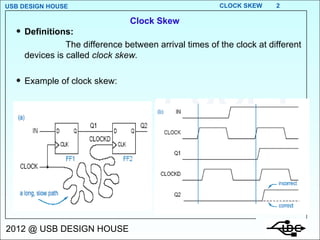
- 2. Clock Skew Definitions: The difference between arrival times of the clock at different devices is called clock skew. Example of clock skew:
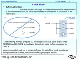
- 3. Clock Skew Buffering the clock: In a large system, the single clock signal may not have adequate fanout to drive all of the devices, so it may be necessary to provide one or two copies of the clock signal. The buffering method of figure (a) produces excessive clock skew, since CLOCK1 and CLOCK2 are delayed through an extra buffer compared to CLOCK. A recommended method is shown in figure (b). All of the clock signals go through identical buffers, and thus have roughly equal delays.
- 4. Minimizing the clock skew Add Delay in Data Path: The amount of the inserted delay (number of BUFD or INVD macros) in the data path should be large enough so that the delay becomes sufficiently greater than the clock skew.
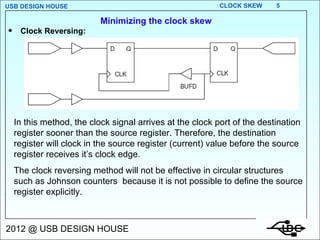
- 5. Minimizing the clock skew Clock Reversing: In this method, the clock signal arrives at the clock port of the destination register sooner than the source register. Therefore, the destination register will clock in the source register (current) value before the source register receives itâs clock edge. The clock reversing method will not be effective in circular structures such as Johnson counters because it is not possible to define the source register explicitly.
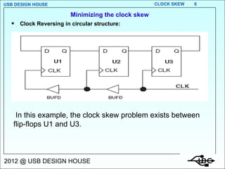
- 6. Minimizing the clock skew Clock Reversing in circular structure: In this example, the clock skew problem exists between flip-flops U1 and U3.
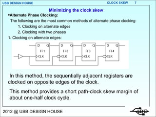
- 7. Minimizing the clock skew Alternate Phase Clocking: The following are the most common methods of alternate phase clocking: 1. Clocking on alternate edges 2. Clocking with two phases 1. Clocking on alternate edges: In this method, the sequentially adjacent registers are clocked on opposite edges of the clock. This method provides a short path-clock skew margin of about one-half clock cycle.
- 8. Minimizing the clock skew Signal propagation for previous circuit:
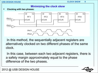
- 9. Minimizing the clock skew Clocking with two phases: In this method, the sequentially adjacent registers are alternatively clocked on two different phases of the same clock. In this case, between each two adjacent registers, there is a safety margin approximately equal to the phase difference of the two phases.
- 10. THANK YOU