Clock Skew 2
5 likes4,382 views
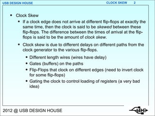
Clock skew refers to differences in the arrival times of a clock signal at different flip-flops. Clock skew is caused by differences in delays along the paths from the clock generator to each flip-flop due to factors like wire lengths, gates, and clock edge inversion. The amount of clock skew affects calculations for the maximum clock frequency and allowable clock skew depends on the minimum setup and hold times of the flip-flops.
1 of 22

Ad
Recommended
Clock Skew 1
Clock Skew 1rchovatiya
Ěý
Clock skew refers to the difference in arrival times of a clock signal at different devices. Excessive clock skew can be minimized by buffering the clock signal so that all signals experience equal delays, adding delay to the data path to account for skew, reversing the clock signal direction to clock the destination register before the source, or using alternate phase clocking with two clock phases or opposite clock edges between sequential registers.Design for Testability
Design for Testability kumar gavanurmath
Ěý
The document discusses design for testability (DFT) techniques. It explains that DFT is important for testing integrated circuits due to unavoidable manufacturing defects. DFT aims to increase testability by making internal nodes more controllable and observable. Common DFT techniques mentioned include adding scan chains, which allow testing at speed by launching test vectors from a shift register. Stuck-at fault and transition fault models are discussed as well as methods for detecting these faults including launch-on-capture and launch-on-shift. Fault equivalence and collapsing techniques are also summarized.Multi mode multi corner (mmmc)
Multi mode multi corner (mmmc)shaik sharief
Ěý
This document discusses multi mode multi corner (MMMC) analysis for chip design. It defines that a mode is a set of design parameters like clocks and timing constraints, and a corner captures process, voltage, and temperature variations. It provides examples of multiple modes like normal, sleep, and test modes and corners for temperature, voltage, process variations, and parasitic interconnects. The document gives an example of analyzing a chip with 4 modes under 3 process-voltage-temperature corners and 3 parasitic interconnect corners, showing 9 analysis cases.Timing Analysis
Timing Analysisrchovatiya
Ěý
The document discusses static timing analysis which is used to verify that logic circuits meet timing requirements. It analyzes different types of timing paths like pad-to-pad, pad-to-setup, clock-to-pad. Static timing analysis is preferred over dynamic analysis for verifying timings in large designs due to faster run times. An example shows calculating maximum frequency of operation by analyzing all path delays in a circuit.Scan insertion
Scan insertionkumar gavanurmath
Ěý
The document discusses the importance of scan design in sequential systems, detailing the operations of scan chains, scannability rules, and scan insertion processes. It elaborates on issues that can prevent proper scan insertion, such as uncontrollable clocks and feedback loops, and presents solutions to these issues. Additionally, it highlights the need for scan compression technology to manage increasingly complex defects and improve testing efficiency.Actel fpga
Actel fpgaAnish Gupta
Ěý
The document discusses Field Programmable Gate Arrays (FPGAs) and compares them to Application-Specific Integrated Circuits (ASICs), highlighting advantages such as quick configuration and reconfigurability, and disadvantages like larger space requirements and slower performance compared to ASICs. It also details the architecture of FPGAs, including components such as configurable logic blocks and input/output blocks, and identifies two types of FPGAs: reprogrammable and one-time programmable. Additionally, it touches on Actel FPGAs, emphasizing their multiplexer-based logic cells and various logic modules.ATPG Methods and Algorithms
ATPG Methods and AlgorithmsDeiptii Das
Ěý
The document discusses various ATPG (Automatic Test Pattern Generation) methods and algorithms. It provides an introduction to ATPG, explaining that ATPG generates test patterns to detect faults in circuits. It then covers major ATPG classifications like pseudorandom, ad-hoc, and algorithmic. Several algorithmic ATPG methods are described, including the D-algorithm, PODEM, FAN, and genetic algorithms. Sequential ATPG is more complex due to memory elements. The summary reiterates that testing large circuits is difficult and many ATPG methods have been developed for combinational and sequential circuits.Fault Simulation (Testing of VLSI Design)
Fault Simulation (Testing of VLSI Design)Usha Mehta
Ěý
This document provides an overview of fault simulation for testing VLSI designs. It discusses:
- The major steps of fault simulation including generating random patterns, simulating the fault-free circuit output, inserting faults, and simulating the faulty circuit output.
- Types of circuit simulators including event-driven, cycle-based, and compiled code simulators.
- Techniques for gate evaluation in simulators like truth tables, input scanning, and input counting.
- The goals of fault simulation as measuring test pattern effectiveness, guiding test pattern generation, and generating fault dictionaries.Automatic Test Pattern Generation (Testing of VLSI Design)
Automatic Test Pattern Generation (Testing of VLSI Design)Usha Mehta
Ěý
The document discusses various methods for automatic test pattern generation (ATPG) in testing VLSI circuits, including:
1) Exhaustive and pseudo-exhaustive methods that test all possible patterns but are infeasible for large circuits.
2) Random and weighted random methods that provide confidence in detecting faults but quality depends on the circuit.
3) Deterministic methods like Boolean difference that compute test vectors to detect specific faults more efficiently than examining all vectors.
4) ATPG uses a two-phase approach - random pattern generation and fault simulation initially to detect many faults easily, followed by targeted deterministic pattern generation to detect remaining faults.Dft (design for testability)
Dft (design for testability)shaik sharief
Ěý
DFT (design for testability) is a technique that facilitates making a design testable after production by adding extra logic during the design process. This extra logic helps with post-production testing. DFT is needed because manufacturing processes are not perfect and can introduce defects. Methods like adding scan chains are used, where scanned flip-flops are connected in series to form a shift register and improve controllability and observability for testing. Common fault models tested for include stuck-at faults, where a line is stuck at either a 0 or 1 value due to defects introduced during manufacturing.Physical design
Physical design Mantra VLSI
Ěý
The document outlines the comprehensive processes and components involved in VLSI physical design, including various types of integrations, design flows, physical design transformations, and data preparation steps. Key concepts like floor planning, placement, timing analysis, and verification methods are discussed, indicating their essential roles in chip manufacturing. Additionally, the document provides detailed terminology, design checks, and considerations for ensuring successful physical design outcomes.VLSI routing
VLSI routingNaveen Kumar
Ěý
The document discusses the routing problem in integrated circuit design, focusing on global and detailed routing techniques. It highlights the objectives, challenges, and methodologies involved in routing nets, including the use of Steiner trees and various types of routing methods such as channel and switchbox routing. The importance of effective routing algorithms is emphasized due to the complexities arising from advancements in IC integration.Understanding cts log_messages
Understanding cts log_messagesMujahid Mohammed
Ěý
Clock tree synthesis log messages provide information about:
1) Preprocessing steps like design updates, buffer characterization, and clock tree constraints.
2) The clock tree synthesis process which includes clustering, meeting timing targets, and reporting results.
3) Post processing steps like embedded clock tree optimization, DRC fixing, and placement legalization.System on Chip (SoC)
System on Chip (SoC)Dimas Ruliandi
Ěý
The document discusses system-on-chip (SoC) design, highlighting its architecture, components, and applications. It emphasizes the challenges of design complexity, time-to-market, and verification requirements, while showcasing the benefits of integrating various components onto a single chip. Additionally, it covers strategies for overcoming design difficulties and references relevant academic resources.Sta by usha_mehta
Sta by usha_mehtaUsha Mehta
Ěý
The document presents content from a webinar on timing analysis in VLSI design, discussing both static and dynamic timing analysis methodologies. It covers critical concepts such as timing verification, the identification of critical paths, delays in circuits, and setup/hold times essential for ensuring proper timing constraints in digital designs. Key techniques and limitations in timing analysis are also explored, emphasizing the importance of accurate assessment of path delays for optimizing VLSI design performance.Physical Design Flow Challenges at 28nm on Multi-million Gate Blocks
Physical Design Flow Challenges at 28nm on Multi-million Gate BlockseInfochips (An Arrow Company)
Ěý
The document discusses the physical design challenges associated with 28nm ASIC technology, covering areas like floorplanning, congestion, timing, and runtime issues encountered during design implementation. It emphasizes the importance of understanding design intricacies, utilizing flow diagrams, and suggests methods for optimizing placement and improving efficiency in complex designs. The conclusion highlights that while 28nm technology presents challenges, effective strategies and tools can significantly enhance designer productivity.Intellectual property in vlsi
Intellectual property in vlsiSaransh Choudhary
Ěý
Intellectual property (IP) in VLSI design refers to reusable logic or functionality units that can be licensed and used as building blocks in chip designs. There are two main types of IP: hard IP, which includes a pre-designed layout, and soft IP, which is delivered as synthesizable code. Soft IP is more vulnerable to theft since it is in a synthesizable form. Memories are often delivered as hard IP since they require careful analog design and peripheral circuitry to be useful. IP differs from custom chip design in that it is created before a specific use, with the goal of reuse across multiple designs. The IP lifecycle involves initial creation through specification, design, testing, and documentation, followed by integration into13 static timing_analysis_4_set_up_and_hold_time_violation_remedy
13 static timing_analysis_4_set_up_and_hold_time_violation_remedyUsha Mehta
Ěý
The document discusses static timing analysis concepts including set-up time, hold time, timing violations, and techniques for fixing violations. It provides examples of how delays are considered in an ideal case without set-up/hold times versus cases with set-up/hold times. Methods for calculating maximum clock frequency and identifying violations are described. Ways to address violations including adjusting buffering, cell sizing, and placement are outlined. The role of static timing analysis in ASIC design flows is also summarized.Define Width and Height of Core and Die (http://www.vlsisystemdesign.com/PD-F...
Define Width and Height of Core and Die (http://www.vlsisystemdesign.com/PD-F...VLSI SYSTEM Design
Ěý
The document discusses the physical aspects of chip design, focusing on the area of core and die, and how to calculate the utilization factor and aspect ratio based on a given netlist. It highlights the importance of grouping standard cells and flip-flops, and assigning dimensions to understand their spatial arrangements on a silicon wafer. Additionally, it explains how varying dimensions impact the utilization and shape of the chip design.dft
dftNejeh Ferjani
Ěý
The document discusses a two-day training on design for testability using Synopsys' DFT Compiler and TetraMAX tools. Day 1 covers basic DFT concepts and techniques including scan path insertion and memory wrappers using DFT Compiler. Day 2 focuses on TetraMAX for fault simulation, modeling memories, and debugging problems.Jtag presentation
Jtag presentationklinetik
Ěý
JTAG (Joint Test Action Group) is a standard interface that allows testing and debugging of printed circuit boards and embedded systems. It enables boundary scan testing which allows control and observation of pin states without physical test probes. The JTAG standard defines a Test Access Port with four pins for control and data. This allows instructions and test data to be serially loaded to test interconnects and perform built-in self-tests of chips on the board. Boundary scan cells are included in JTAG chips to intercept pin states for testing.Metastability,MTBF,synchronizer & synchronizer failure
Metastability,MTBF,synchronizer & synchronizer failureprashant singh
Ěý
This document discusses metastability, mean time between failures (MTBF), synchronizers, and synchronizer failures. It begins with introductions to metastability and cases where it can occur. It then illustrates metastability with diagrams and graphs. It discusses how systems enter metastability and what occurs during metastability. The document derives the MTBF equation and provides an example calculation. It concludes by listing references for further information.Synchronous and asynchronous clock
Synchronous and asynchronous clockNallapati Anindra
Ěý
The document discusses synchronous and asynchronous clocks. A clock is a square wave signal generated by an oscillator that provides two levels, high and low. Clocks are used to time signals in circuits to avoid glitches, which are unpredictable outputs caused by differences in propagation delays. There are two types of clocks: synchronous clocks have the same phase but frequencies may differ, while asynchronous clocks have different phases and frequencies may also differ. Asynchronous clocks can cause glitches, so synchronization is needed to make clocks operate synchronously.Design for testability and automatic test pattern generation
Design for testability and automatic test pattern generationDilip Mathuria
Ěý
The document discusses Design for Testability (DFT) and automatic test pattern generation, emphasizing the importance of making integrated circuit designs more testable and cost-effective. It covers various DFT methods, including ad-hoc, structured methods like scan design, and Built-In Self-Test (BIST), alongside the economic implications of testing at various production stages. Additionally, it details fault models such as stuck-at faults, bridging faults, and the principles of automatic test pattern generation to enhance testing efficiency and effectiveness.VLSI-Physical Design- Tool Terminalogy
VLSI-Physical Design- Tool TerminalogyMurali Rai
Ěý
The physical design flow begins with placement which involves assigning exact locations to modules like gates and standard cells to minimize area and interconnect cost while meeting timing constraints, with the goal of enabling easier routing; placement tools take as input the netlist, floorplan, libraries, and constraints to perform global and detailed placement as well as optimization. The quality of placement significantly impacts the ability to route the design successfully.Deterministic Test Pattern Generation ( D-Algorithm of ATPG) (Testing of VLSI...
Deterministic Test Pattern Generation ( D-Algorithm of ATPG) (Testing of VLSI...Usha Mehta
Ěý
The document discusses deterministic test pattern generation (ATPG) for combinational circuits. It provides an overview of ATPG algorithms and concepts like fault excitation, propagation, and justification. Hard and easy faults are defined based on the difficulty of controlling inputs and observing outputs. Testability measures like controllability and observability are introduced to analyze fault difficulty. Developing one's own ATPG tool is discussed, along with ideas for future extensions.Vlsi testing
Vlsi testingDilip Mathuria
Ěý
This document discusses VLSI faults and testing. It begins by outlining the VLSI realization process from customer needs to fabrication. It then defines key terms like defects, faults, errors and describes common types of defects from fabrication. The document discusses logical fault models and the role of testing in detecting errors. It outlines different types of testing like production testing and burn-in testing. Finally, it discusses topics like design for testability, fault simulation, and benefits of testing like improved quality and economy of scale.ASIC VS FPGA.ppt
ASIC VS FPGA.pptgopakumar885691
Ěý
FPGAs were introduced in 1984 as a programmable alternative to PLDs. They fill the gap between discrete logic and smaller PLDs on the low end and more expensive ASICs on the high end. The basic elements of an FPGA are configurable logic blocks (CLBs), configurable I/O blocks (IOBs), and a programmable interconnect. FPGAs from vendors like Xilinx and Altera have a regular architecture of CLBs surrounded by IOBs and connected via a hierarchy of programmable interconnects.file (1).ppt
file (1).pptAbhimanyu159566
Ěý
This document discusses timing considerations in sequential circuits, including:
1. Defining timing parameters like maximum clock frequency, clock skew, and global setup and hold times based on flip-flop and gate delays.
2. Explaining why gating the clock signal to control loading is a poor design practice due to potential unintended triggering of flip-flops.
3. Calculating maximum clock frequency based on critical paths, showing the impact of clock skew and logic delays between flip-flops.Cadence Conformal Logic Equivalance Check
Cadence Conformal Logic Equivalance CheckBharathwajThirumalai
Ěý
The document discusses the timing and constraints involved in sequential digital network design, emphasizing setup and hold time requirements for flip-flops. It details the relationships between clock signals and data stability, and how violations can affect system reliability. The lecture concludes with a focus on the need for design adjustments and retiming to optimize performance and meet timing constraints.More Related Content
What's hot (20)
Automatic Test Pattern Generation (Testing of VLSI Design)
Automatic Test Pattern Generation (Testing of VLSI Design)Usha Mehta
Ěý
The document discusses various methods for automatic test pattern generation (ATPG) in testing VLSI circuits, including:
1) Exhaustive and pseudo-exhaustive methods that test all possible patterns but are infeasible for large circuits.
2) Random and weighted random methods that provide confidence in detecting faults but quality depends on the circuit.
3) Deterministic methods like Boolean difference that compute test vectors to detect specific faults more efficiently than examining all vectors.
4) ATPG uses a two-phase approach - random pattern generation and fault simulation initially to detect many faults easily, followed by targeted deterministic pattern generation to detect remaining faults.Dft (design for testability)
Dft (design for testability)shaik sharief
Ěý
DFT (design for testability) is a technique that facilitates making a design testable after production by adding extra logic during the design process. This extra logic helps with post-production testing. DFT is needed because manufacturing processes are not perfect and can introduce defects. Methods like adding scan chains are used, where scanned flip-flops are connected in series to form a shift register and improve controllability and observability for testing. Common fault models tested for include stuck-at faults, where a line is stuck at either a 0 or 1 value due to defects introduced during manufacturing.Physical design
Physical design Mantra VLSI
Ěý
The document outlines the comprehensive processes and components involved in VLSI physical design, including various types of integrations, design flows, physical design transformations, and data preparation steps. Key concepts like floor planning, placement, timing analysis, and verification methods are discussed, indicating their essential roles in chip manufacturing. Additionally, the document provides detailed terminology, design checks, and considerations for ensuring successful physical design outcomes.VLSI routing
VLSI routingNaveen Kumar
Ěý
The document discusses the routing problem in integrated circuit design, focusing on global and detailed routing techniques. It highlights the objectives, challenges, and methodologies involved in routing nets, including the use of Steiner trees and various types of routing methods such as channel and switchbox routing. The importance of effective routing algorithms is emphasized due to the complexities arising from advancements in IC integration.Understanding cts log_messages
Understanding cts log_messagesMujahid Mohammed
Ěý
Clock tree synthesis log messages provide information about:
1) Preprocessing steps like design updates, buffer characterization, and clock tree constraints.
2) The clock tree synthesis process which includes clustering, meeting timing targets, and reporting results.
3) Post processing steps like embedded clock tree optimization, DRC fixing, and placement legalization.System on Chip (SoC)
System on Chip (SoC)Dimas Ruliandi
Ěý
The document discusses system-on-chip (SoC) design, highlighting its architecture, components, and applications. It emphasizes the challenges of design complexity, time-to-market, and verification requirements, while showcasing the benefits of integrating various components onto a single chip. Additionally, it covers strategies for overcoming design difficulties and references relevant academic resources.Sta by usha_mehta
Sta by usha_mehtaUsha Mehta
Ěý
The document presents content from a webinar on timing analysis in VLSI design, discussing both static and dynamic timing analysis methodologies. It covers critical concepts such as timing verification, the identification of critical paths, delays in circuits, and setup/hold times essential for ensuring proper timing constraints in digital designs. Key techniques and limitations in timing analysis are also explored, emphasizing the importance of accurate assessment of path delays for optimizing VLSI design performance.Physical Design Flow Challenges at 28nm on Multi-million Gate Blocks
Physical Design Flow Challenges at 28nm on Multi-million Gate BlockseInfochips (An Arrow Company)
Ěý
The document discusses the physical design challenges associated with 28nm ASIC technology, covering areas like floorplanning, congestion, timing, and runtime issues encountered during design implementation. It emphasizes the importance of understanding design intricacies, utilizing flow diagrams, and suggests methods for optimizing placement and improving efficiency in complex designs. The conclusion highlights that while 28nm technology presents challenges, effective strategies and tools can significantly enhance designer productivity.Intellectual property in vlsi
Intellectual property in vlsiSaransh Choudhary
Ěý
Intellectual property (IP) in VLSI design refers to reusable logic or functionality units that can be licensed and used as building blocks in chip designs. There are two main types of IP: hard IP, which includes a pre-designed layout, and soft IP, which is delivered as synthesizable code. Soft IP is more vulnerable to theft since it is in a synthesizable form. Memories are often delivered as hard IP since they require careful analog design and peripheral circuitry to be useful. IP differs from custom chip design in that it is created before a specific use, with the goal of reuse across multiple designs. The IP lifecycle involves initial creation through specification, design, testing, and documentation, followed by integration into13 static timing_analysis_4_set_up_and_hold_time_violation_remedy
13 static timing_analysis_4_set_up_and_hold_time_violation_remedyUsha Mehta
Ěý
The document discusses static timing analysis concepts including set-up time, hold time, timing violations, and techniques for fixing violations. It provides examples of how delays are considered in an ideal case without set-up/hold times versus cases with set-up/hold times. Methods for calculating maximum clock frequency and identifying violations are described. Ways to address violations including adjusting buffering, cell sizing, and placement are outlined. The role of static timing analysis in ASIC design flows is also summarized.Define Width and Height of Core and Die (http://www.vlsisystemdesign.com/PD-F...
Define Width and Height of Core and Die (http://www.vlsisystemdesign.com/PD-F...VLSI SYSTEM Design
Ěý
The document discusses the physical aspects of chip design, focusing on the area of core and die, and how to calculate the utilization factor and aspect ratio based on a given netlist. It highlights the importance of grouping standard cells and flip-flops, and assigning dimensions to understand their spatial arrangements on a silicon wafer. Additionally, it explains how varying dimensions impact the utilization and shape of the chip design.dft
dftNejeh Ferjani
Ěý
The document discusses a two-day training on design for testability using Synopsys' DFT Compiler and TetraMAX tools. Day 1 covers basic DFT concepts and techniques including scan path insertion and memory wrappers using DFT Compiler. Day 2 focuses on TetraMAX for fault simulation, modeling memories, and debugging problems.Jtag presentation
Jtag presentationklinetik
Ěý
JTAG (Joint Test Action Group) is a standard interface that allows testing and debugging of printed circuit boards and embedded systems. It enables boundary scan testing which allows control and observation of pin states without physical test probes. The JTAG standard defines a Test Access Port with four pins for control and data. This allows instructions and test data to be serially loaded to test interconnects and perform built-in self-tests of chips on the board. Boundary scan cells are included in JTAG chips to intercept pin states for testing.Metastability,MTBF,synchronizer & synchronizer failure
Metastability,MTBF,synchronizer & synchronizer failureprashant singh
Ěý
This document discusses metastability, mean time between failures (MTBF), synchronizers, and synchronizer failures. It begins with introductions to metastability and cases where it can occur. It then illustrates metastability with diagrams and graphs. It discusses how systems enter metastability and what occurs during metastability. The document derives the MTBF equation and provides an example calculation. It concludes by listing references for further information.Synchronous and asynchronous clock
Synchronous and asynchronous clockNallapati Anindra
Ěý
The document discusses synchronous and asynchronous clocks. A clock is a square wave signal generated by an oscillator that provides two levels, high and low. Clocks are used to time signals in circuits to avoid glitches, which are unpredictable outputs caused by differences in propagation delays. There are two types of clocks: synchronous clocks have the same phase but frequencies may differ, while asynchronous clocks have different phases and frequencies may also differ. Asynchronous clocks can cause glitches, so synchronization is needed to make clocks operate synchronously.Design for testability and automatic test pattern generation
Design for testability and automatic test pattern generationDilip Mathuria
Ěý
The document discusses Design for Testability (DFT) and automatic test pattern generation, emphasizing the importance of making integrated circuit designs more testable and cost-effective. It covers various DFT methods, including ad-hoc, structured methods like scan design, and Built-In Self-Test (BIST), alongside the economic implications of testing at various production stages. Additionally, it details fault models such as stuck-at faults, bridging faults, and the principles of automatic test pattern generation to enhance testing efficiency and effectiveness.VLSI-Physical Design- Tool Terminalogy
VLSI-Physical Design- Tool TerminalogyMurali Rai
Ěý
The physical design flow begins with placement which involves assigning exact locations to modules like gates and standard cells to minimize area and interconnect cost while meeting timing constraints, with the goal of enabling easier routing; placement tools take as input the netlist, floorplan, libraries, and constraints to perform global and detailed placement as well as optimization. The quality of placement significantly impacts the ability to route the design successfully.Deterministic Test Pattern Generation ( D-Algorithm of ATPG) (Testing of VLSI...
Deterministic Test Pattern Generation ( D-Algorithm of ATPG) (Testing of VLSI...Usha Mehta
Ěý
The document discusses deterministic test pattern generation (ATPG) for combinational circuits. It provides an overview of ATPG algorithms and concepts like fault excitation, propagation, and justification. Hard and easy faults are defined based on the difficulty of controlling inputs and observing outputs. Testability measures like controllability and observability are introduced to analyze fault difficulty. Developing one's own ATPG tool is discussed, along with ideas for future extensions.Vlsi testing
Vlsi testingDilip Mathuria
Ěý
This document discusses VLSI faults and testing. It begins by outlining the VLSI realization process from customer needs to fabrication. It then defines key terms like defects, faults, errors and describes common types of defects from fabrication. The document discusses logical fault models and the role of testing in detecting errors. It outlines different types of testing like production testing and burn-in testing. Finally, it discusses topics like design for testability, fault simulation, and benefits of testing like improved quality and economy of scale.ASIC VS FPGA.ppt
ASIC VS FPGA.pptgopakumar885691
Ěý
FPGAs were introduced in 1984 as a programmable alternative to PLDs. They fill the gap between discrete logic and smaller PLDs on the low end and more expensive ASICs on the high end. The basic elements of an FPGA are configurable logic blocks (CLBs), configurable I/O blocks (IOBs), and a programmable interconnect. FPGAs from vendors like Xilinx and Altera have a regular architecture of CLBs surrounded by IOBs and connected via a hierarchy of programmable interconnects.Define Width and Height of Core and Die (http://www.vlsisystemdesign.com/PD-F...
Define Width and Height of Core and Die (http://www.vlsisystemdesign.com/PD-F...VLSI SYSTEM Design
Ěý
Similar to Clock Skew 2 (20)
file (1).ppt
file (1).pptAbhimanyu159566
Ěý
This document discusses timing considerations in sequential circuits, including:
1. Defining timing parameters like maximum clock frequency, clock skew, and global setup and hold times based on flip-flop and gate delays.
2. Explaining why gating the clock signal to control loading is a poor design practice due to potential unintended triggering of flip-flops.
3. Calculating maximum clock frequency based on critical paths, showing the impact of clock skew and logic delays between flip-flops.Cadence Conformal Logic Equivalance Check
Cadence Conformal Logic Equivalance CheckBharathwajThirumalai
Ěý
The document discusses the timing and constraints involved in sequential digital network design, emphasizing setup and hold time requirements for flip-flops. It details the relationships between clock signals and data stability, and how violations can affect system reliability. The lecture concludes with a focus on the need for design adjustments and retiming to optimize performance and meet timing constraints.07_Digital timing_&_Pipelining.ppt
07_Digital timing_&_Pipelining.pptBUCHUPALLIVIMALAREDD2
Ěý
This document discusses timing analysis of logic circuits. It defines propagation delay time (tp) as the time required for an output signal to change due to a change in the input signal. A timing diagram is used to graphically represent tp. The document discusses how real circuits have intrinsic resistance and capacitance that cause delay. It provides an example of calculating delay through a simple RC circuit. Combinational logic delay is represented using a cloud model. The document also discusses setup time, hold time, and register delay time for D flip-flops and how to calculate maximum switching frequency, including using pipelining to increase maximum frequency.Timing notes 2006
Timing notes 2006pavan kumar
Ěý
This document discusses timing parameters for combinational and sequential logic circuits. It defines propagation delay and contamination delay for combinational logic, and propagation delay, contamination delay, setup time, and hold time for sequential logic circuits like flip-flops. It also discusses determining maximum clock frequency for sequential circuits based on these timing parameters, modeling delays from gates and interconnect, using clock trees, and issues related to clock skew and jitter.Fast020702
Fast020702Abdo sayed
Ěý
This document contains the agenda for a workshop on Multi-Gbps TCP. The workshop includes presentations on high speed networks, LHC networks, TCP/AQM protocols and their duality model, control theory and stability of TCP/AQM, FAST simulations, and related TCP kernel projects. Presentations will be given by researchers from Caltech, CERN, UCLA, and INRIA on topics such as TCP protocols, active queue management, stability analysis, and simulations. There will also be discussion periods following some of the presentations.Contamination delay
Contamination delayNima Afraz
Ěý
Contamination delay (tcd) refers to the amount of time needed for a change in a logic input to result in an initial change at an output of combinational logic. It guarantees that the output will not change in response to an input change within tcd time units. For sequential logic, tcd indicates the time needed for a change in the flip-flop clock input to result in an initial change at the flip-flop output. Ensuring inputs are stable for the specified setup time before and hold time after the clock prevents metastability in flip-flops. The determination of a circuit's tcd requires identifying the shortest path of contamination delays from input to output.Ece4510 notes10
Ece4510 notes10K. M. Shahrear Hyder
Ěý
This document discusses digital implementation of analog controllers. There are three main approaches to digitizing an analog controller: 1) emulation using the forward rectangular rule to approximate derivatives with differences, 2) emulation using the backward rectangular rule, and 3) emulation using the bilinear rule. The zero-order hold operation in the digital to analog conversion introduces an effective delay that degrades the emulated system's performance compared to the original analog controller. Faster sampling reduces the impact of this delay.Te442 lecture02-2016-14-4-2016-1
Te442 lecture02-2016-14-4-2016-1colman mboya
Ěý
This document discusses timing considerations for digital electronics systems using standard integrated circuits (ICs). It covers propagation delay, which is the time it takes for a change on an input to propagate to the output. Sequential circuits like flip-flops only change value in response to a clock signal, so their timing parameters are specified relative to the rising or falling edge of the clock. The maximum clock frequency of a sequential circuit can be determined by analyzing the propagation delays of its components and ensuring all timing requirements are met.Timing analysis
Timing analysisKunal Doshi
Ěý
The paper discusses a new approach to static timing analysis in integrated circuits, emphasizing the importance of timing checks for the functionality of combinational and sequential circuits. It differentiates between various types of delays including propagation, setup, and hold times, as well as the impact of clock skew on circuit performance. By analyzing timing paths and delays, the paper aims to ensure accurate circuit design and prevent timing-related issues such as setup and hold violations.How to time logic
How to time logicDhruv Thakkar
Ěý
This document discusses various techniques for timing logic in digital design, including reducing logic delay through boolean algebra, Karnaugh maps, identifying and resolving long and critical paths, pipelining, simulation, and static timing analysis. It defines important timing terms like setup time, hold time, clock skew, and describes challenges like meeting timing constraints while avoiding race conditions. The goal is to optimize the logic such that it can be timed according to requirements and meet the specified clock period slack.Timing analysis
Timing analysiskhldun said
Ěý
The document discusses timing analysis concepts such as propagation delay, contamination delay, glitches, setup time constraints, hold time constraints, clock skew, metastability, and timing analysis terminology. Propagation delay is the maximum time for an output to reach its final value after an input changes, while contamination delay is the minimum time for an output to start changing after an input changes. Setup and hold time constraints ensure inputs are stable for long enough before and after the clock edge. Clock skew accounts for differences in clock signal arrival times. Metastability can cause unpredictable behavior if signals change too close to the clock edge.Pda capwap - frank rausche
Pda capwap - frank rauschecfpbolivia
Ěý
The document discusses high strain pile testing using the Pile Driving Analyzer (PDA) system. It outlines how the PDA measures strain, acceleration, force and velocity during pile driving to evaluate forces and stresses in piles, integrity, bearing capacity and resistance. It provides examples of PDA testing results and discusses problems that can be identified. The PDA and CAPWAP methods are described for analyzing test results to determine pile capacity and resistance distributions.2.5 pda-capwap - gray
2.5 pda-capwap - graycfpbolivia
Ěý
The document discusses high strain pile testing using a Pile Driving Analyzer (PDA) system. It provides an overview of PDA testing methodology, including measuring strain and acceleration at the pile top to determine forces and stresses in the pile. It also describes using PDA data to evaluate pile integrity, bearing capacity, and resistance distribution. The document outlines PDA capabilities such as remote monitoring and analyzing restrike data. It further explains the Case Method for determining static pile capacity from PDA measurements.Chapter 08
Chapter 08Khalid Hasan
Ěý
This document discusses different methods for implementing counters and time delays using an 8085 microprocessor. It provides examples of using a single register, register pair, and nested loops to create time delays. Calculations are shown for determining the delay based on the clock frequency, number of clock cycles in the loop, and value loaded into the delay register. An illustrative problem is presented to count from 0 to 9 with a one second delay between each count using modulo 10 counting.CAPACITIVE SENSORS ELECTRICAL WAFER SORT
CAPACITIVE SENSORS ELECTRICAL WAFER SORTMassimo Garavaglia
Ěý
This document discusses testing capacitive sensors using electrical measurements. It describes an electrical model of a capacitive sensor and how its capacitance varies with applied bias voltage. Methods are presented for testing for leakage currents, measuring the capacitance-voltage relationship, and determining the sensor's dynamic behavior by analyzing its resonant frequency and quality factor. Requirements for the test setup include using a capacitance meter, waveform generator, and digitizer configured for Fourier analysis to isolate the sensor's motional signal from background terms in its output current spectrum. Calibration procedures are also outlined to compensate for stray capacitances in the test circuit.·ˇłľ˛ú±đ»ĺ»ĺ±đ»ĺłĺł§˛â˛őłŮ±đłľ˛őłĺ˛ő±đł¦´Ç˛Ô»ĺł¦´ÇłÜ°ů˛ő±đłĺ±«˛Ôľ±±ą±đ°ů˛őľ±łŮĂ©°Ő´ÇłÜ±ô´ÇłÜ˛ő±đ.±č»ĺ´Ú
·ˇłľ˛ú±đ»ĺ»ĺ±đ»ĺłĺł§˛â˛őłŮ±đłľ˛őłĺ˛ő±đł¦´Ç˛Ô»ĺł¦´ÇłÜ°ů˛ő±đłĺ±«˛Ôľ±±ą±đ°ů˛őľ±łŮĂ©°Ő´ÇłÜ±ô´ÇłÜ˛ő±đ.±č»ĺ´ÚTinhinaneAitMessaoud
Ěý
2e cours de systemes embarquésQuartz Crystal Oscillators and Phase-Locked Loops
Quartz Crystal Oscillators and Phase-Locked LoopsADVA
Ěý
The document is a tutorial on quartz crystal oscillators (XO) and phase-locked loops (PLL), detailing their technologies, categories, and characteristics. It explains the principles of quartz crystal oscillation, including temperature sensitivity and different oscillator types, as well as the functioning of PLLs, their transfer functions, and applications. Additionally, it addresses the physical layer support for telecom timing applications and the implications of various oscillator types in this context.Fmax Analysis
Fmax Analysisrchovatiya
Ěý
The maximum clock frequency for a synchronous sequential circuit is limited by the timing parameters of its flip-flops and gates. These parameters include propagation delays, setup times, and hold times. The minimum clock period is the reciprocal of the maximum clock frequency. For a specific 7474 circuit, the maximum clock period must be greater than or equal to 60 ns to account for the propagation delays and setup time of the flip-flops.Standard cells library design
Standard cells library designBharat Biyani
Ěý
This document describes the design and characterization of a D flip-flop cell. It includes the layout, schematic, simulation waveforms, and timing analysis of the D flip-flop. The layout uses two metal layers and occupies an area of 76.8 ÎĽm2. Timing parameters such as setup time, clock-to-output time, and delay are calculated through HSPICE simulation and optimization curves.·ˇłľ˛ú±đ»ĺ»ĺ±đ»ĺłĺł§˛â˛őłŮ±đłľ˛őłĺ˛ő±đł¦´Ç˛Ô»ĺł¦´ÇłÜ°ů˛ő±đłĺ±«˛Ôľ±±ą±đ°ů˛őľ±łŮĂ©°Ő´ÇłÜ±ô´ÇłÜ˛ő±đ.±č»ĺ´Ú
·ˇłľ˛ú±đ»ĺ»ĺ±đ»ĺłĺł§˛â˛őłŮ±đłľ˛őłĺ˛ő±đł¦´Ç˛Ô»ĺł¦´ÇłÜ°ů˛ő±đłĺ±«˛Ôľ±±ą±đ°ů˛őľ±łŮĂ©°Ő´ÇłÜ±ô´ÇłÜ˛ő±đ.±č»ĺ´ÚTinhinaneAitMessaoud
Ěý
Ad
Clock Skew 2
- 1. Clock Skew
- 2. Clock Skew If a clock edge does not arrive at different flip-flops at exactly the same time, then the clock is said to be skewed between these flip-flops. The difference between the times of arrival at the flip-flops is said to be the amount of clock skew . Clock skew is due to different delays on different paths from the clock generator to the various flip-flops. Different length wires (wires have delay) Gates (buffers) on the paths Flip-Flops that clock on different edges (need to invert clock for some flip-flops) Gating the clock to control loading of registers (a very bad idea)
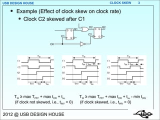
- 3. Example (Effect of clock skew on clock rate) Clock C2 skewed after C1 T W ≥ max T PFF + max t OR + t su (if clock not skewed, i.e., t INV = 0) T W ≥ max T PFF + max t OR + t su - min t INV (if clock skewed, i.e., t INV > 0)
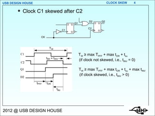
- 4. Clock C1 skewed after C2 T W ≥ max T PFF + max t OR + t su (if clock not skewed, i.e., t INV = 0) T W ≥ max T PFF + max t OR + t su + max t INV (if clock skewed, i.e., t INV > 0)
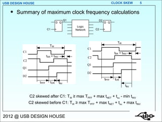
- 5. Summary of maximum clock frequency calculations C2 skewed after C1: T W ≥ max T PFF + max t NET + t su - min t INV C2 skewed before C1: T W ≥ max T PFF + max t NET + t su + max t INV
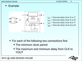
- 6. Example For each of the following two connections find The minimum clock period The maximum and minimum delay from CLK to YOUT
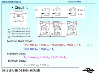
- 7. Circuit 1: max t PFF + max t QY + (n-2) max t XY +max t XD + t su max t PFF + max t QD + t su n ≥ 2 Tw ≥ Tw ≥ ≥ T W Minimum Clock Period: Maximum Delay: Minimum Delay: T CY ≤ T CY ≥ max t PFF + max t QY + (n-1) max t XY min t PFF + min t QY
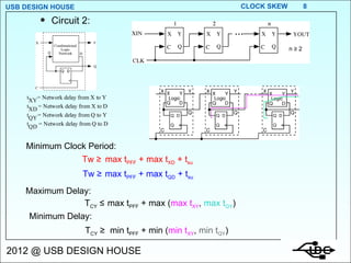
- 8. Circuit 2: n ≥ 2 max t PFF + max t XD + t su max t PFF + max t QD + t su Tw ≥ Tw ≥ Minimum Clock Period: Maximum Delay: Minimum Delay: T CY ≤ T CY ≥ max t PFF + max ( max t XY , max t QY ) min t PFF + min ( min t XY , min t QY )
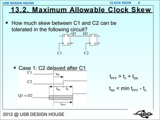
- 9. 13.2. Maximum Allowable Clock Skew How much skew between C1 and C2 can be tolerated in the following circuit? Case 1: C2 delayed after C1 t PFF > t h + t SK t SK < min t PFF - t h
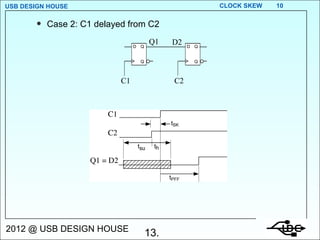
- 10. Case 2: C1 delayed from C2 13.
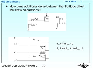
- 11. How does additional delay between the flip-flops affect the skew calculations? 13. t SK ≤ min t PFF - t h t sk ≤ min t PFF + min t MUX - t h
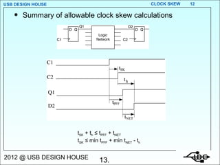
- 12. Summary of allowable clock skew calculations 13. t SK + t h ≤ t PFF + t NET t SK ≤ min t PFF + min t NET - t h
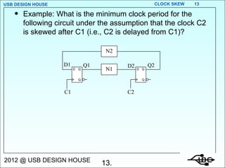
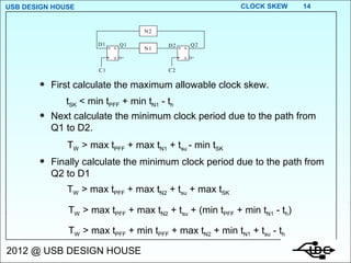
- 13. Example: What is the minimum clock period for the following circuit under the assumption that the clock C2 is skewed after C1 (i.e., C2 is delayed from C1)? 13.
- 14. First calculate the maximum allowable clock skew. Next calculate the minimum clock period due to the path from Q1 to D2. Finally calculate the minimum clock period due to the path from Q2 to D1 t SK < min t PFF + min t N1 - t h T W > max t PFF + max t N1 + t su - min t SK T W > max t PFF + max t N2 + t su + max t SK T W > max t PFF + max t N2 + t su + (min t PFF + min t N1 - t h ) T W > max t PFF + min t PFF + max t N2 + min t N1 + t su - t h N 1 N 2 C 1 C 2 Q 1 D 2 Q 2 D 1 D Q Q D Q Q
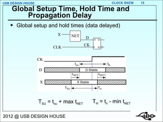
- 15. Global Setup Time, Hold Time and Propagation Delay Global setup and hold times (data delayed) T SU = t su + max t NET T H = t h - min t NET
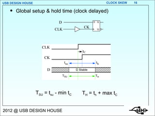
- 16. Global setup & hold time (clock delayed) T SU = t su - min t C T H = t h + max t C
- 17. Global setup & hold time (data & clock delayed) T SU = t su + max t NET - min t C T H = t h - min t NET + max t C
- 18. Global propagation delay T P = t C + t FF + t NET
- 19. Example Find T SU and T H for input signal LD relative to CLK. T SU = t su +max t NET - min t C T H = t h - min t NET + max t C = t su + max t INV + max t NAND + max t NAND - min t INV = t h - min t NAND - min t NAND + max T INV
- 20. Tips & Tricks Use timing diagrams to determine the timing properties of sequential circuits Pitfalls Using typical timing values from the data sheet (use only max and/or min values) Gating the clock
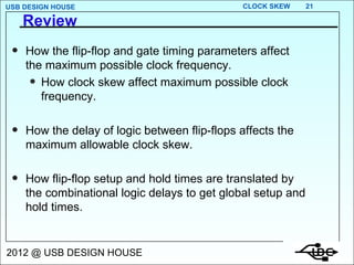
- 21. Review How the flip-flop and gate timing parameters affect the maximum possible clock frequency. How clock skew affect maximum possible clock frequency. How the delay of logic between flip-flops affects the maximum allowable clock skew. How flip-flop setup and hold times are translated by the combinational logic delays to get global setup and hold times.
- 22. THANK YOU