


![2D Stencil Computation
? ╣╠Č©źčź┐®`ź¾ż╦żĶż├żŲźŪ®`ź┐ź╗ź├ź╚ż╬Ė³ą┬ż“ąąż”Ę┤Å═ėŗ╦Ń
? Ų½╬óĘųĘĮ│╠╩Įż╬Į³╦ŲĮŌż“Ū¾żßżļ╩ųĘ©ż╬1ż─
? (e.g. ¤ß┴”覯¼┴„╠Õ┴”覯¼ļŖ┤┼Ü▌覿╩ż╔)
v1[i][j] =
(C0 * v0[i-1][j]) + (C1 * v0[i][j+1]) +
(C2 * v0[i][j-1]) + (C3 * v0[i+1][j]);
v1[i][j]żŽ4Į³░°ż╬éÄż“ūŃżĘ║Žż’ż╗żļż│ż╚ż╦żĶż├żŲėŗ╦ŃżĄżņżļ
C0, C1, C2, C3: ųžż▀Č©╩²
Time-step k
Update data set
3](https://image.slidesharecdn.com/reconf-130130023300-phpapp02/85/IEICE-technical-report-RECONF-January-2013-4-320.jpg)


![Stencil Computation at MADD
? v1[i][j] = (C0 * v0[i-1][j]) + (C1 * v0[i][j-1]) + (C2 *
v0[i][j+1]) + (C3 * v0[i+1][j]);
8-stages
8-stages
19](https://image.slidesharecdn.com/reconf-130130023300-phpapp02/85/IEICE-technical-report-RECONF-January-2013-20-320.jpg)
![Stencil Computation at MADD
? v1[i][j] = (C0 * v0[i-1][j]) + (C1 * v0[i][j-1]) + (C2 *
v0[i][j+1]) + (C3 * v0[i+1][j]);
C0
8-stages
8-stages
20](https://image.slidesharecdn.com/reconf-130130023300-phpapp02/85/IEICE-technical-report-RECONF-January-2013-21-320.jpg)
![Stencil Computation at MADD
? v1[i][j] = (C0 * v0[i-1][j]) + (C1 * v0[i][j-1]) + (C2 *
v0[i][j+1]) + (C3 * v0[i+1][j]);
C1
8-stages
Take 8 cycles
8-stages
21](https://image.slidesharecdn.com/reconf-130130023300-phpapp02/85/IEICE-technical-report-RECONF-January-2013-22-320.jpg)
![Stencil Computation at MADD
? v1[i][j] = (C0 * v0[i-1][j]) + (C1 * v0[i][j-1]) + (C2 *
v0[i][j+1]) + (C3 * v0[i+1][j]);
C1
8-stages
8-stages
22](https://image.slidesharecdn.com/reconf-130130023300-phpapp02/85/IEICE-technical-report-RECONF-January-2013-23-320.jpg)
![Stencil Computation at MADD
? v1[i][j] = (C0 * v0[i-1][j]) + (C1 * v0[i][j-1]) + (C2 *
v0[i][j+1]) + (C3 * v0[i+1][j]);
C2
8-stages
Take 8 cycles
8-stages
Take 8 cycles
23](https://image.slidesharecdn.com/reconf-130130023300-phpapp02/85/IEICE-technical-report-RECONF-January-2013-24-320.jpg)
![Stencil Computation at MADD
? v1[i][j] = (C0 * v0[i-1][j]) + (C1 * v0[i][j-1]) + (C2 *
v0[i][j+1]) + (C3 * v0[i+1][j]);
C2
8-stages
8-stages
24](https://image.slidesharecdn.com/reconf-130130023300-phpapp02/85/IEICE-technical-report-RECONF-January-2013-25-320.jpg)
![Stencil Computation at MADD
? v1[i][j] = (C0 * v0[i-1][j]) + (C1 * v0[i][j-1]) + (C2 *
v0[i][j+1]) + (C3 * v0[i+1][j]);
C3
8-stages
8-stages
25](https://image.slidesharecdn.com/reconf-130130023300-phpapp02/85/IEICE-technical-report-RECONF-January-2013-26-320.jpg)
![Stencil Computation at MADD
? v1[i][j] = (C0 * v0[i-1][j]) + (C1 * v0[i][j-1]) + (C2 *
v0[i][j+1]) + (C3 * v0[i+1][j]);
8-stages
8-stages
26](https://image.slidesharecdn.com/reconf-130130023300-phpapp02/85/IEICE-technical-report-RECONF-January-2013-27-320.jpg)
![Stencil Computation at MADD
? v1[i][j] = (C0 * v0[i-1][j]) + (C1 * v0[i][j-1]) + (C2 *
v0[i][j+1]) + (C3 * v0[i+1][j]);
8-stages
8-stages
V1[i][j] 27](https://image.slidesharecdn.com/reconf-130130023300-phpapp02/85/IEICE-technical-report-RECONF-January-2013-28-320.jpg)


![ź»źĒź├ź»ż╬ż║żņż╬Ų└ü²(3/3)
£yČ©Ģrķg[sec] ūŅÉÖż╬ż║żņ ż║żņż╬ś╦£╩Ų½▓Ņ
[ppm]
20 20.47(x=3, y=5) 4.73
x=1
1.50 x=2
cycle variea on / M ccycle
1.00 x=3
0.50 40 20.47(x=3, y=5) 4.68
0.00 x=4
-0.50 1 x=5
-1.00 2
3
4 x=6
-1.50
-2.00
5
6
80 20.47(x=3, y=5) 4.73
x=8 x=7
-2.50 7
8 x=7
-3.00 x=8
x=6
-3.50
x=5
-4.00
x=4
160 20.59(x=3, y=5) 4.77
x=3
x=2
x=1
320 20.66(x=3, y=5) 4.79
320Ż¾ecż╬ź»źĒź├ź»ż╬ż║żņż“20sec
ż╬ź»źĒź├ź»ż╬ż║żņżŪĖŅż├ż┐ź░źķźš
Ė„£yČ©Ģrķgż╦ż¬ż▒żļūŅÉÖż╬ż║żņż╚ż║żņż╬ś╦£╩Ų½▓Ņ
?ź»źĒź├ź»ż╬ż║żņżŽŻ¼Ģrķgż╦żŽę└┤µżĘż╩żżż│ż╚ż“┤_šJ
Ī·Ģrķg▌S╔ŽżŪżŽż█ż▄ēõ╗»żĘż╩żżź»źĒź├ź»ż╬ż║żņż“┐╝æ]żĘż┐źĘź╣źŲźÓįOėŗż¼▒žę¬
41](https://image.slidesharecdn.com/reconf-130130023300-phpapp02/85/IEICE-technical-report-RECONF-January-2013-42-320.jpg)


![Performance of Single FPGA Node(1/2)
? Grid-sizeŻ║64Ī┴128
? IterationŻ║500,000
? Performance and Power Consumption(160MHz)
? PerformanceŻ║2.24GFlop/s
? Power ConsumptionŻ║2.37W
Peak performance[GFlop/s]
Peak = 2Ī┴FĪ┴NFPGAĪ┴NMADDĪ┴7/8
PeakŻ║Peak performance[GFlop/s]
FŻ║Operation frequency[GHz]
NFPGAŻ║the number of FPGA
NMADDŻ║the number of MADD
7/8: Average utilization of MADD unit
Ī· The four multiplications and the three additions
v1[i][j] = (C0 * v0[i-1][j]) + (C1 * v0[i][j+1]) +
(C2 * v0[i][j-1]) + (C3 * v0[i+1][j]);
48](https://image.slidesharecdn.com/reconf-130130023300-phpapp02/85/IEICE-technical-report-RECONF-January-2013-49-320.jpg)


IEICE technical report (RECONF), January 2013.
- 1. 2013/01/17 źĻź│ź¾źšźŻź«źŃźķźųźļźĘź╣źŲźÓ蹊┐╗ß FPGAėŗ╦ŃÅĻė├ (15:15-15:40) ░k▒Ē20Ęų + ┘|ę╔ÅĻ┤5Ęų źßź├źĘźÕĮėŠAFPGAźóźņ®`ż“ė├żżż┐ Ė▀ąį─▄ź╣źŲź¾źĘźļėŗ╦ŃÖCż╬įOėŗż╚īgū░ ĪŅąĪ┴ų šÅŲĮ?1 Ė▀Ū░╠’Ż©╔ĮŲķŻ® ╔ņę▓?1 ?2 ╝¬×ü ųtČ■?1 ?1 ¢|Š®╣żśI┤¾č¦ ┤¾č¦į║Ūķł¾└Ē╣żč¦čąŠ┐┐Ų ?2 ╚š▒Šč¦ągš±┼d╗ß ╠žäe蹊┐åTŻ©DC1Ż®
- 2. ░k▒Ēż╬┴„żņ ? ╣¾▒╩│ę┤Īźóźņ®`ż╦ż¬ż▒żļź╣źŲź¾źĘźļ╝Ų╦Ń ? źóźņ®`ķg═©ą┼ż╬ūŅ▀m╗» ? č▌╦Ńźµź╦ź├ź╚ż╬źŪ®`ź┐äI└Ē ? FPGAźóźņ®`źĘź╣źŲźÓż╬å¢Ņ}ĄŃ ? ź»źĒź├ź»ż╬żążķż─żŁż╬Č©┴┐įuü² ? ═¼Ų┌╗·╣╣ż╬╔Ķ╝Ų?īgū░ ? ąį─▄įuü²?ĮYšō 1
- 3. ░k▒Ēż╬┴„żņ ? ╣¾▒╩│ę┤Īźóźņ®`ż╦ż¬ż▒żļź╣źŲź¾źĘźļ╝Ų╦Ń ? źóźņ®`ķg═©ą┼ż╬ūŅ▀m╗» ? č▌╦Ńźµź╦ź├ź╚ż╬źŪ®`ź┐äI└Ē ? FPGAźóźņ®`źĘź╣źŲźÓż╬å¢Ņ}ĄŃ ? ź»źĒź├ź»ż╬żążķż─żŁż╬Č©┴┐įuü² ? ═¼Ų┌╗·╣╣ż╬╔Ķ╝Ų?īgū░ ? ąį─▄įuü²?ĮYšō 2
- 4. 2D Stencil Computation ? ╣╠Č©źčź┐®`ź¾ż╦żĶż├żŲźŪ®`ź┐ź╗ź├ź╚ż╬Ė³ą┬ż“ąąż”Ę┤Å═ėŗ╦Ń ? Ų½╬óĘųĘĮ│╠╩Įż╬Į³╦ŲĮŌż“Ū¾żßżļ╩ųĘ©ż╬1ż─ ? (e.g. ¤ß┴”覯¼┴„╠Õ┴”覯¼ļŖ┤┼Ü▌覿╩ż╔) v1[i][j] = (C0 * v0[i-1][j]) + (C1 * v0[i][j+1]) + (C2 * v0[i][j-1]) + (C3 * v0[i+1][j]); v1[i][j]żŽ4Į³░°ż╬éÄż“ūŃżĘ║Žż’ż╗żļż│ż╚ż╦żĶż├żŲėŗ╦ŃżĄżņżļ C0, C1, C2, C3: ųžż▀Č©╩² Time-step k Update data set 3
- 5. ╣¾▒╩│ę┤Īźóźņ®`ż╦ż¬ż▒żļź╣źŲź¾źĘźļ╝Ų╦Ń Ż║Ė±ūėĄŃ FPGA FPGA FPGA FPGA PROM SRAM PROM SRAM PROM SRAM PROM SRAM FPGA FPGA FPGA FPGA PROM SRAM PROM SRAM PROM SRAM PROM SRAM FPGA FPGA FPGA FPGA PROM SRAM PROM SRAM PROM SRAM PROM SRAM FPGA FPGA FPGA FPGA PROM SRAM PROM SRAM PROM SRAM PROM SRAM ?źŪ®`ź┐ź╗ź├ź╚żŽFPGAż╬╩²ż╦ÅĻżĖżŲĘųĖŅżĄżņŻ¼Ė±╝{żĄżņżļ ?Ė„FPGAżŽüK┴ąż╦ź╣źŲź¾źĘźļėŗ╦Ńż“īgąąż╣żļ 4
- 6. ScalableCore System *Takamaeda-Yamazaki, S., (ARC 2012) (2012). ? ąĪ╚▌┴┐FPGAż“č}╩²ė├żżż┐ź┐źżźļą═źó®`źŁźŲź»ź┴źŃźĘź▀źÕźņ®`ź┐ ? źßź╦®`ź│źóźūźĒź╗ź├źĄż╬Ė▀╦┘źĘź▀źÕźņ®`ź┐ ? ż│ż╬źĘź╣źŲźÓż╬źŽ®`ź╔ź”ź¦źóż“HPCźŽ®`ź╔ź”ź¦źóźóź»ź╗źķźņ®`ź┐ż╬╗∙ ĄAż╚żĘżŲ╩╣ė├ One FPGA node FPGA PROM SRAM 5
- 7. ░k▒Ēż╬┴„żņ ? ╣¾▒╩│ę┤Īźóźņ®`ż╦ż¬ż▒żļź╣źŲź¾źĘźļ╝Ų╦Ń ? źóźņ®`ķg═©ą┼ż╬ūŅ▀m╗» ? č▌╦Ńźµź╦ź├ź╚ż╬źŪ®`ź┐äI└Ē ? FPGAźóźņ®`źĘź╣źŲźÓż╬å¢Ņ}ĄŃ ? ź»źĒź├ź»ż╬żążķż─żŁż╬Č©┴┐įuü² ? ═¼Ų┌╗·╣╣ż╬╔Ķ╝Ų?īgū░ ? ąį─▄įuü²?ĮYšō 6
- 8. Ė„╣¾▒╩│ę┤Īż╦ż¬ż▒żļĖ±ūėĄŃż╬╝Ų╦Ń╦│ą“ ╠ß░Ė╩ųĘ© ?FPGAż¼╔ŽŽ┬ż╦ĮėŠAżĘż┐ż╚żŁż╬ėŗ╦ŃĒśą“ż“▒╚▌^ż╣żļ ?╬ęĪ®ż╬╠ß░Ė╩ųĘ©żŽįS╚▌żŪżŁżļ═©ą┼źņźżźŲź¾źĘż“ēł╝ėżĄż╗żļ 7
- 9. Comparison between (a) and (b) (1/2) ?źżźŲźņ®`źĘźńź¾ : ╚½żŲż╬Ė±ūėĄŃż“1Č╚ėŗ╦Ńż╣żļż┐żßż╬äI└Ē ?║åģgż╬ż┐żßŻ¼éÄż╬Ė³ą┬żŽż½ż½żļźĄźżź»źļ╩²żŽ1ż╚ż╣żļ ?Ė„FPGA żŽĖŅżĻĄ▒żŲżķżņż┐Ė±ūėĄŃ16 éĆż╬éÄż“Ė„źżźŲźņ®`źĘźńź¾ż┤ż╚Ė³ą┬ż╣żļ Ż©Ė±ūėĄŃ0ż½żķ15żžż╬ĒśĘ¼żŪĖ³ą┬ż╣żļŻ® A0 A1 A2 A3 C12 C13 C14 C15 FPGA(A) FPGA(C) A4 A5 A6 A7 C8 C9 C10 C11 A8 A9 A10 A11 C4 C5 C6 C7 A12 B0 A13 B1 A14 B2 A15 B3 vs C0 D0 C1 D1 C2 D2 C3 D3 FPGA(B) FPGA(D) B4 B5 B6 B7 D4 D5 D6 D7 B8 B9 B10 B11 D8 D9 D10 D11 B12 B13 B14 B15 D12 D13 D14 D15 (a) (b) Proposed method 8
- 10. Comparison between (a) and (b) (2/2) A0 A1 A2 A3 First Iteration end 0 16 FPGA(A) A4 A5 A6 A7 A8 A9 A10 A11 A0 A1 A2 A3 A4 A5 A6 A7 A8 A9 A10 A11 A12 A13 A14 A15 A0 A1 A12 A13 A14 A15 ĪŁ B0 B1 B2 B3 B4 B5 B6 B7 B8 B9 B10 B11 B12 B13 B14 B15 B0 B1 B0 B1 B2 B3 FPGA(B) B4 B5 B6 B7 B8 B9 B10 B11 (a) B12 B13 B14 B15 Proposed C12 C13 C14 C15 0 First Iteration end 16 method FPGA(C) C8 C9 C10 C11 C0 C1 C2 C3 C4 C5 C6 C7 C8 C9 C10 C11 C12 C13 C14 C15 C0 C1 C4 C5 C6 C7 ĪŁ D0 D1 D2 D3 D4 D5 D6 D7 D8 D9 D10 D11 D12 D13 D14 D15 D0 D1 C0 C1 C2 C3 D0 D1 D2 D3 FPGA(D) D4 D5 D6 D7 D8 D9 D10 D11 (b) D12 D13 D14 D15 9
- 11. Comparison between (a) and (b) (2/2) A0 A1 A2 A3 First Iteration end 0 16 FPGA(A) A4 A5 A6 A7 A8 A9 A10 A11 A0 A1 A2 A3 A4 A5 A6 A7 A8 A9 A10 A11 A12 A13 A14 A15 A0 A1 A12 A13 A14 A15 ĪŁ B0 B1 B2 B3 B4 B5 B6 B7 B8 B9 B10 B11 B12 B13 B14 B15 B0 B1 B0 B1 B2 B3 In order not to stall the computation FPGA(B) B4 B5 B6 B7 of B1, the value of A13 must be B8 B9 B10 B11 communicated within three cycles (a) B12 B13 B14 B15 (14, 15, 16) after the computationĪŁ Proposed C12 C13 C14 C15 0 First Iteration end 16 method FPGA(C) C8 C9 C10 C11 C0 C1 C2 C3 C4 C5 C6 C7 C8 C9 C10 C11 C12 C13 C14 C15 C0 C1 C4 C5 C6 C7 ĪŁ D0 D1 D2 D3 D4 D5 D6 D7 D8 D9 D10 D11 D12 D13 D14 D15 D0 D1 C0 C1 C2 C3 D0 D1 D2 D3 FPGA(D) D4 D5 D6 D7 D8 D9 D10 D11 (b) D12 D13 D14 D15 10
- 12. Comparison between (a) and (b) (2/2) A0 A1 A2 A3 First Iteration end 0 16 FPGA(A) A4 A5 A6 A7 A8 A9 A10 A11 A0 A1 A2 A3 A4 A5 A6 A7 A8 A9 A10 A11 A12 A13 A14 A15 A0 A1 A12 A13 A14 A15 ĪŁ B0 B1 B2 B3 B4 B5 B6 B7 B8 B9 B10 B11 B12 B13 B14 B15 B0 B1 B0 B1 B2 B3 In order not to stall the computation FPGA(B) B4 B5 B6 B7 of B1, the value of A13 must be B8 B9 B10 B11 communicated within three cycles (a) B12 B13 B14 B15 (14, 15, 16) after the computationĪŁ Proposed C12 C13 C14 C15 0 First Iteration end 16 method FPGA(C) C8 C9 C10 C11 C0 C1 C2 C3 C4 C5 C6 C7 C8 C9 C10 C11 C12 C13 C14 C15 C0 C1 C4 C5 C6 C7 ĪŁ D0 D1 D2 D3 D4 D5 D6 D7 D8 D9 D10 D11 D12 D13 D14 D15 D0 D1 C0 C1 C2 C3 D0 D1 D2 D3 FPGA(D) D4 D5 D6 D7 In order not to stall the D8 D9 D10 D11 computation of D1 of Iteration 2 (17th cycle), the margin to send (b) D12 D13 D14 D15 11 value of C1 (1st cycle) is 15 cycles
- 13. Comparison between (a) and (b) (NĪ┴M grid-points) N If the NĪ┴M grid-points are assigned to a single FPGA, every shared value must be communicated within N©C1cycles FPGA M Iteration end ĪŁ ĪŁ FPGA (a) N-1 cycles If the NĪ┴M grid-points are assigned to a Proposed N single FPGA, every shared value must be method communicated within NĪ┴M©C1cycles FPGA M Iteration end ĪŁ ĪŁ FPGA NĪ┴M-1 cycles 12 (b)
- 14. Computing Order Applied Proposed Method Ż║computation order ? ż│ż╬╠ß░Ė╩ųĘ©ż╦żĶżĻ╝s1źżźŲźņ®`źĘźńź¾ż╬įS╚▌żŪżŁżļ═©ą┼źņźżźŲź¾źĘż“┤_▒Ż ? Ė±ūėĄŃż╬╩²ż¼ēł╝ėż╣żļż█ż╔Ż¼įS╚▌żŪżŁżļ═©ą┼źņźżźŲź¾źĘżŽź╣ź▒®`źļż╣żļ 13
- 15. ░k▒Ēż╬┴„żņ ? ╣¾▒╩│ę┤Īźóźņ®`ż╦ż¬ż▒żļź╣źŲź¾źĘźļ╝Ų╦Ń ? źóźņ®`ķg═©ą┼ż╬ūŅ▀m╗» ? č▌╦Ńźµź╦ź├ź╚ż╬źŪ®`ź┐äI└Ē ? FPGAźóźņ®`źĘź╣źŲźÓż╬å¢Ņ}ĄŃ ? ź»źĒź├ź»ż╬żążķż─żŁż╬Č©┴┐įuü² ? ═¼Ų┌╗·╣╣ż╬╔Ķ╝Ų?īgū░ ? ąį─▄įuü²?ĮYšō 14
- 16. System Architecture Configura on ROM XCF04S Ser/Des North Clock FPGA Spartan-6 Reset Sync mux2 Memory unit (BlockRAMs) W 0 1 2 3 4 5 6 7 E Computation unit 0 1 2 3 4 5 6 7 0 1 2 3 4 5 6 7 (Multiply and Adder) mux mux mux mux mux mux mux mux MADD MADD MADD MADD MADD MADD MADD MADD Ser/Des Ser/Des West East mux8 South Ser/Des 15
- 17. Relationship between The Data Subset and BlockRAM(Memory unit) BlockRAM: low-latency SRAM which each FPGA has. FPGA array 4Ī┴4 BlockRAMs (Data is assigned) The data set which assigned to each FPGA is split in the vertical direction, and is stored in each BlockRAM (0Ī½7) If the data set of 64Ī┴128 is assigned to one FPGA, the split data set (8Ī┴128) is stored in each BlockRAM (0Ī½7). 16
- 18. Relationship between MADD and BlockRAM(Memory unit) ?The data set stored in each BlockRAM is computed by each MADD. ?Each MADD performs the computation in parallel. ?The computed data is stored in BlockRAM. 17
- 19. MADD Architecture(Computation unit) ? MADD ? Multiply: seven pipeline stages ? Adder: seven pipeline stages ? Both multiply and adder are single precision floating-point unit which conforms to IEEE 754. 18
- 20. Stencil Computation at MADD ? v1[i][j] = (C0 * v0[i-1][j]) + (C1 * v0[i][j-1]) + (C2 * v0[i][j+1]) + (C3 * v0[i+1][j]); 8-stages 8-stages 19
- 21. Stencil Computation at MADD ? v1[i][j] = (C0 * v0[i-1][j]) + (C1 * v0[i][j-1]) + (C2 * v0[i][j+1]) + (C3 * v0[i+1][j]); C0 8-stages 8-stages 20
- 22. Stencil Computation at MADD ? v1[i][j] = (C0 * v0[i-1][j]) + (C1 * v0[i][j-1]) + (C2 * v0[i][j+1]) + (C3 * v0[i+1][j]); C1 8-stages Take 8 cycles 8-stages 21
- 23. Stencil Computation at MADD ? v1[i][j] = (C0 * v0[i-1][j]) + (C1 * v0[i][j-1]) + (C2 * v0[i][j+1]) + (C3 * v0[i+1][j]); C1 8-stages 8-stages 22
- 24. Stencil Computation at MADD ? v1[i][j] = (C0 * v0[i-1][j]) + (C1 * v0[i][j-1]) + (C2 * v0[i][j+1]) + (C3 * v0[i+1][j]); C2 8-stages Take 8 cycles 8-stages Take 8 cycles 23
- 25. Stencil Computation at MADD ? v1[i][j] = (C0 * v0[i-1][j]) + (C1 * v0[i][j-1]) + (C2 * v0[i][j+1]) + (C3 * v0[i+1][j]); C2 8-stages 8-stages 24
- 26. Stencil Computation at MADD ? v1[i][j] = (C0 * v0[i-1][j]) + (C1 * v0[i][j-1]) + (C2 * v0[i][j+1]) + (C3 * v0[i+1][j]); C3 8-stages 8-stages 25
- 27. Stencil Computation at MADD ? v1[i][j] = (C0 * v0[i-1][j]) + (C1 * v0[i][j-1]) + (C2 * v0[i][j+1]) + (C3 * v0[i+1][j]); 8-stages 8-stages 26
- 28. Stencil Computation at MADD ? v1[i][j] = (C0 * v0[i-1][j]) + (C1 * v0[i][j-1]) + (C2 * v0[i][j+1]) + (C3 * v0[i+1][j]); 8-stages 8-stages V1[i][j] 27
- 29. MADD Pipeline Operation(Computation unit) ? The computation of grid-points 11Ī½18 8-stages InputŻ▓(adder) 8-stages Input1(adder) 28
- 30. MADD Pipeline Operation (in cycles 0?7) ? The computation of grid-points 11Ī½18 8 7 6 5 The grid-points 1Ī½8 are loaded from 4 3 BlockRAM and they are input to the 2 1 multiplier in cycles 0Ī½7. 8-stages InputŻ▓(adder) 8-stages Input1(adder) 29
- 31. MADD Pipeline Operation (in cycles 8?15) ? The computation of grid-points 11Ī½18 17 16 15 14 13 The computation result is output from 12 11 multiplier, at the same times, grid-points 10 10Ī½17 are input to the multiplier in 8 8-stages 7 cycles 8Ī½15. 6 5 4 3 InputŻ▓(adder) 2 8-stages 1 Input1(adder) 30
- 32. MADD Pipeline Operation (in cycles 16?23) ? The computation of grid-points 11Ī½18 19 18 17 16 The grid-points 12Ī½19 are input to the 15 14 multiplier, at the same time, value of grid- 13 12 points 1?8 and 10Ī½17 multiplied by a 8 17 7 16 8-stages weighting factor are summed in cycles 16Ī½ 6 15 5 14 23. 4 13 3 12 2 11 8-stages InputŻ▓(adder) 1 10 Input1(adder) 31
- 33. MADD Pipeline Operation (in cycles 24?31) ? The computation of grid-points 11Ī½18 28 27 26 25 Input2(adder): 1Ī½8 and 10Ī½17 grid-points 8 17 24 23 Input1(adder): 12Ī½19 grid-points 7 16 22 21 6 15 Input(multiplier): 21Ī½28 grid-points 19 8-stages 5 14 18 13 17 4 InputŻ▓(adder) 3 16 12 15 2 11 14 1 10 13 8-stages 12 Input1(adder) 32
- 34. MADD Pipeline Operation (in cycles 32?39) ? The computation of grid-points 11Ī½18 18 17 16 15 Input2(adder): 1Ī½8, 10Ī½17 and 12Ī½19 grid-points 8 17 19 14 13 Input1(adder): 21Ī½28 grid-points 7 16 18 12 11 Input(multiplier): 11Ī½18 grid-points 6 15 17 28 5 14 16 27 8-stages 4 13 15 26 InputŻ▓(adder) 25 3 12 14 24 2 11 13 23 1 10 12 22 21 8-stages Input1(adder) 33
- 35. MADD Pipeline Operation (in cycles 40?48) ? The computation of grid-points 11Ī½18 27 26 25 24 The computation results that data of up, down, 23 22 left and right gird-points are multiplied by a 21 18 20 17 weighting factor and summed are output in 16 cycles 40Ī½48. 15 8-stages 14 13 InputŻ▓(adder) 12 11 8 17 19 28 8-stages 7 16 18 27 6 15 17 26 5 14 16 25 4 13 15 Input1(adder) 24 3 12 14 23 2 11 13 22 1 10 12 21 34
- 36. MADD Pipeline Operation(Computation unit) ?The filing rate of the pipeline: (N-8/N)Ī┴100% (N is cycles which taken this computation.) ? Achievement of high computation performance and the small circuit area ? This scheduling is valid only when width of computed grid is equal to the pipeline stages of multiplier and adder. 35
- 37. ░k▒Ēż╬┴„żņ ? ╣¾▒╩│ę┤Īźóźņ®`ż╦ż¬ż▒żļź╣źŲź¾źĘźļ╝Ų╦Ń ? źóźņ®`ķg═©ą┼ż╬ūŅ▀m╗» ? č▌╦Ńźµź╦ź├ź╚ż╬źŪ®`ź┐äI└Ē ? FPGAźóźņ®`źĘź╣źŲźÓż╬å¢Ņ}ĄŃ ? ź»źĒź├ź»ż╬żążķż─żŁż╬Č©┴┐įuü² ? ═¼Ų┌╗·╣╣ż╬╔Ķ╝Ų?īgū░ ? ąį─▄įuü²?ĮYšō 36
- 38. FPGAźóźņ®`źĘź╣źŲźÓż╬å¢Ņ}ĄŃ ? ż│ż╬FPGAźóźņ®`źĘź╣źŲźÓżŽź░źĒ®`źąźļź»źĒź├ź»ż“ėążĘżŲżżż╩żżŻĪ ? Ė„ź╬®`ź╔żŽ╣╠ėąż╬ź»źĒź├ź»ź╔źßźżź¾ż“│ųż├żŲżżżļ ?ź╬®`ź╔╩²ż“ēł╝ėżĄż╗ż┐Ģrż╦Ż¼ėŗ╦ŃÖCż╬▓╗Š▀║Žż“░kęŖŻĪ ?Ė„FPGAź╬®`ź╔ż╬ź»źĒź├ź»ų▄Ų┌ż╬żążķż─żŁż¼įŁę“Ż┐Ż┐ ? ź»źĒź├ź»ų▄Ų┌ż╬ż║żņż“Č©┴┐Ą─ż╦įuü² ? ėŗ╦ŃÖCż¼ķLĢrķgŻ¼░▓Č©żĘżŲäėū„ż╣żļż┐żßż╬ÖCśŗż“įOėŗ?īgū░ 37
- 39. ź»źĒź├ź»ź¬źĘźņ®`ź┐ (CSX-750PB(B)) ? Ė„FPGAź╬®`ź╔ż╦┤Ņ▌d (40MHz) ? ų▄▓©╩²░▓Č©Č╚Ż║Ī└50ppmęį─┌ż“▒Żį^ ? 1,000,000źĄźżź»źļżŪż║żņżļźĄźżź»źļżŽĪ└50źĄźżź»źļęį─┌ ? Ė„FPGAź╬®`ź╔ż╬ź»źĒź├ź»ż╬ż║żņżŽŻ¼ų▄▓©╩²░▓Č©Č╚ż╬éÄż╦żĶ ż├żŲū¾ė꿥żņżļ CSX-750PB(B) 38
- 40. ź»źĒź├ź»ż╬ż║żņż╬įuü²(1/3) ? ScalableCoreźĘź╣źŲźÓż“└¹ė├ (8Ī┴8śŗ│╔) ? ėŗ£yĢrķgż“ēõ╗»żĄż╗żŲź»źĒź├ź»ż╬ż║żņż“£yČ© Display Power Supply FPGA FPGA FPGA FPGA FPGA FPGA USB Port PROM SRAM PROM SRAM PROM SRAM PROM SRAM PROM SRAM PROM SRAM FPGA FPGA FPGA FPGA FPGA FPGA PROM SRAM PROM SRAM PROM SRAM PROM SRAM PROM SRAM PROM SRAM FPGA FPGA FPGA FPGA FPGA FPGA PROM SRAM PROM SRAM PROM SRAM PROM SRAM PROM SRAM PROM SRAM 39
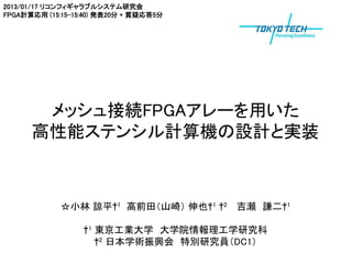
- 41. ź»źĒź├ź»ż╬ż║żņż╬Ų└ü²(2/3) ? X▌SŻ¼Y▌SŻ║Ė„FPGAź╬®`ź╔ż╬ū∙ś╦ ? Z▌S1,000,000źĄźżź»źļżóż┐żĻż╬ź»źĒź├ź»ż╬ż║żņ(ppm) x=1 x=1 x=1 25.00 25.00 25.00 x=2 x=2 x=2 cycle variea on / M ccycle cycle variea on / M ccycle cycle variea on / M ccycle 20.00 x=3 20.00 x=3 20.00 x=3 15.00 x=4 15.00 x=4 15.00 x=4 x=5 10.00 x=5 10.00 x=5 10.00 x=8 x=6 x=7 5.00 x=8 x=6 5.00 x=8 x=6 5.00 x=6 x=7 x=7 x=7 0.00 x=7 0.00 x=7 x=5 x=6 x=6 0.00 1 1 x=4 x=8 -5.00 x=5 x=8 -5.00 x=5 x=8 2 2 1 3 x=4 3 x=4 2 x=3 4 4 3 5 x=3 5 x=3 4 x=2 6 6 5 6 7 x=1 20sec 7 8 x=1 x=2 80sec 7 8 x=1 x=2 320sec 8 £yČ©ĢrķgŻ║20sec £yČ©ĢrķgŻ║80sec £yČ©ĢrķgŻ║80sec ūŅÉÖż╬ż║żņŻ║20.5ppm (x=3, y=5) ūŅÉÖż╬ż║żņŻ║20.5ppm (x=3, y=5) ūŅÉÖż╬ż║żņŻ║20.7ppm (x=3, y=5) ź»źĒź├ź»ż╬żążķż─żŁż╬ś╦£╩Ų½▓ŅŻ║4.73 ź»źĒź├ź»ż╬żążķż─żŁż╬ś╦£╩Ų½▓ŅŻ║4.73 ź»źĒź├ź»ż╬żążķż─żŁż╬ś╦£╩Ų½▓ŅŻ║4.79 ?ų▄▓©╩²░▓Č©Č╚Ī└50ppmż¼▒Żį^żĄżņżŲżżżļż│ż╚ż“┤_šJ 40
- 42. ź»źĒź├ź»ż╬ż║żņż╬Ų└ü²(3/3) £yČ©Ģrķg[sec] ūŅÉÖż╬ż║żņ ż║żņż╬ś╦£╩Ų½▓Ņ [ppm] 20 20.47(x=3, y=5) 4.73 x=1 1.50 x=2 cycle variea on / M ccycle 1.00 x=3 0.50 40 20.47(x=3, y=5) 4.68 0.00 x=4 -0.50 1 x=5 -1.00 2 3 4 x=6 -1.50 -2.00 5 6 80 20.47(x=3, y=5) 4.73 x=8 x=7 -2.50 7 8 x=7 -3.00 x=8 x=6 -3.50 x=5 -4.00 x=4 160 20.59(x=3, y=5) 4.77 x=3 x=2 x=1 320 20.66(x=3, y=5) 4.79 320Ż¾ecż╬ź»źĒź├ź»ż╬ż║żņż“20sec ż╬ź»źĒź├ź»ż╬ż║żņżŪĖŅż├ż┐ź░źķźš Ė„£yČ©Ģrķgż╦ż¬ż▒żļūŅÉÖż╬ż║żņż╚ż║żņż╬ś╦£╩Ų½▓Ņ ?ź»źĒź├ź»ż╬ż║żņżŽŻ¼Ģrķgż╦żŽę└┤µżĘż╩żżż│ż╚ż“┤_šJ Ī·Ģrķg▌S╔ŽżŪżŽż█ż▄ēõ╗»żĘż╩żżź»źĒź├ź»ż╬ż║żņż“┐╝æ]żĘż┐źĘź╣źŲźÓįOėŗż¼▒žę¬ 41
- 43. ░k▒Ēż╬┴„żņ ? ╣¾▒╩│ę┤Īźóźņ®`ż╦ż¬ż▒żļź╣źŲź¾źĘźļ╝Ų╦Ń ? źóźņ®`ķg═©ą┼ż╬ūŅ▀m╗» ? č▌╦Ńźµź╦ź├ź╚ż╬źŪ®`ź┐äI└Ē ? FPGAźóźņ®`źĘź╣źŲźÓż╬å¢Ņ}ĄŃ ? ź»źĒź├ź»ż╬żążķż─żŁż╬Č©┴┐įuü² ? ═¼Ų┌╗·╣╣ż╬╔Ķ╝Ų?īgū░ ? ąį─▄įuü²?ĮYšō 42
- 44. ═¼Ų┌╗·╣╣ż╬╔Ķ╝Ų ? FPGAź╬®`ź╔(A)ż“Masterź╬®`ź╔ż╚Č©┴x ? Ė„FPGAź╬®`ź╔żŽMasterź╬®`ź╔ż½żķ”┴ +”┬ ż╬ų▄Ų┌żŪ╦═ą┼żĄżņżļą┼║┼ż╦═¼Ų┌żĘżŲėŗ╦Ń ż“īgąą ? ═¼Ų┌ą┼║┼ż“╩▄ą┼ż╣żļż▐żŪŻ¼Masterź╬®`ź╔ęį═Ōż╬ź╬®`ź╔żŽėŗ╦Ńż“ź╣ź╚®`źļ synchronize synchronize ”┴ ”┬ ”┴ ”┬ ”┴ ”┬ ”┴ Ż║1 źżźŲźņ®`źĘźńź¾ķgż╦ż¬ż▒ A żļź╣źŲź¾źĘźļėŗ╦Ńż╦ꬿ╣żļźĄ źżź»źļ stall stall stall B ”┬ Ż║Ė„FPGAź╬®`ź╔ż╬ź»źĒź├ź» ż╬ż║żņż“╬³ģ¦ż╣żļź▐®`źĖź¾ C D 43
- 45. ═¼Ų┌ÖCśŗż╬īgū░ ? Ė„FPGAź╬®`ź╔żŽMasterź╬®`ź╔ż½żķ”┴ +”┬ ż╬ų▄Ų┌żŪ╦═ą┼żĄżņżļą┼║┼ż╦═¼Ų┌żĘżŲėŗ╦Ń ż“īgąą ? ═¼Ų┌ą┼║┼ż“╩▄ą┼ż╣żļż▐żŪŻ¼Masterź╬®`ź╔ęį═Ōż╬ź╬®`ź╔żŽėŗ╦Ńż“ź╣ź╚®`źļ ? ą┼║┼ż“╩▄ą┼żĘż┐FPGAź╬®`ź╔żŽ╩²źĄźżź»źļ┤²ż├żŲż½żķŻ¼ū¾ĘĮŽ“ż╚Ž┬ĘĮŽ“ż╦═¼Ų┌ą┼ ║┼ż“╦═ą┼żĘŻ¼ėŗ╦Ńż“į┘ķ_ ”┴ ”┬ A ”┴ ”┬ A B master B for anti-chattering C C D D for anti-chattering 44
- 46. ═¼Ų┌╗·╣╣ż╬Č»ū„Ś╩į^(100ź╬®`ź╔) Coming soon!! 45
- 47. ░k▒Ēż╬┴„żņ ? ╣¾▒╩│ę┤Īźóźņ®`ż╦ż¬ż▒żļź╣źŲź¾źĘźļ╝Ų╦Ń ? źóźņ®`ķg═©ą┼ż╬ūŅ▀m╗» ? č▌╦Ńźµź╦ź├ź╚ż╬źŪ®`ź┐äI└Ē ? FPGAźóźņ®`źĘź╣źŲźÓż╬å¢Ņ}ĄŃ ? ź»źĒź├ź»ż╬żążķż─żŁż╬Č©┴┐įuü² ? ═¼Ų┌╗·╣╣ż╬╔Ķ╝Ų?īgū░ ? ąį─▄įuü²?ĮYšō 46
- 48. Environment (Performance of Single FPGA Node) ? FPGAŻ║Xilinx Spartan-6 XC6SLX16 ? BlockRAM: 64KB ? Design tool: Xilinx ISE webpack 13.3 ? Hardware description language: Verilog HDL ? Implementation of MADDŻ║IP core generated by Xilinx core-generator ? Implementing single MADD expends four pieces of 32 DSP-blocks which a Spartan-6 FPGA has. Ī¾ Therefore, the number of MADD to be able to be implemented in single FPGA is eight SRAM is not used. ScalableCore board 47
- 49. Performance of Single FPGA Node(1/2) ? Grid-sizeŻ║64Ī┴128 ? IterationŻ║500,000 ? Performance and Power Consumption(160MHz) ? PerformanceŻ║2.24GFlop/s ? Power ConsumptionŻ║2.37W Peak performance[GFlop/s] Peak = 2Ī┴FĪ┴NFPGAĪ┴NMADDĪ┴7/8 PeakŻ║Peak performance[GFlop/s] FŻ║Operation frequency[GHz] NFPGAŻ║the number of FPGA NMADDŻ║the number of MADD 7/8: Average utilization of MADD unit Ī· The four multiplications and the three additions v1[i][j] = (C0 * v0[i-1][j]) + (C1 * v0[i][j+1]) + (C2 * v0[i][j-1]) + (C3 * v0[i+1][j]); 48
- 50. Performance of Single FPGA Node(2/2) ? č▌╦Ńąį─▄ (160MHz) ? 2.24GFlop/s 26% of Intel Core i7-2600 (single thread, 3.4GHz, -O3 option) ? ļŖ┴”żóż┐żĻż╬č▌╦Ńąį─▄Ż║0.95GFlop/sW Performance/W value is about six-times better than Nvidia GTX280 GPU card. Nvidia GTX 280 card ? źŽ®`ź╔ź”ź¦źó┘Yį┤╩╣ė├┬╩ ? LUT: 50% ? Slice: 67% ? BlockRAM: 75% ? DSP48A1: 100% 49
- 51. Conclusion ? ź»źĒź├ź»ż╬ż║żņż“Č©┴┐Ą─ż╦įuü² ? ź»źĒź├ź»ż╬ż║żņżŽäėū„Ģrķgż╦ę└┤µżĘż╩żż ? įOėŗż¬żĶżėīgū░ ? Ė„FPGAź╬®`ź╔ż╬╬╗ų├Ūķł¾ż“╚ĪĄ├ż╣żļ╗ž┬Ęż“īgū░ ? Ė„FPGAż¼═¼Ų┌ż╣żļÖCśŗż“īgū░ ? 100ź╬®`ź╔żŪż╬äėū„ż“┤_šJ ? ąį─▄įuü² (One-FPGA node) ? äėū„ų▄▓©╩² 160MHz (no communication) ? īgąąąį─▄ 2.24GFlop/s. Ž¹┘MļŖ┴” 2.37W. ? źŽ®`ź╔ź”ź¦źó┘Yį┤╩╣ė├┬╩ : Slices 67% ? Į±ßßż╬šnŅ} ? FPGAźóźņ®`ż╬ąį─▄įuü² ? Ą═ļŖ┴”ż╦Ž“ż▒ż┐īgū░ 50