


![Moore/Mealy TradeŌĆÉOffs
ŌĆó How are they different?
ŌĆó Moore: outputs = f( state ) only
ŌĆó Mealy outputs = f( state and input )
ŌĆó Mealy outputs generally occur one cycle earlier than a Moore:
Moore: delayed assertion of P Mealy: immediate assertion of P
L L
P P
Clock Clock
State[0] State
ŌĆó Compared to a Moore FSM, a Mealy FSM might...
ŌĆō Be more difficult to conceptualize and design
ŌĆō Have fewer states
9/26/2018 6.111 Fall 2018 18](https://image.slidesharecdn.com/lecture12-220717220532-ddc3038c/85/Lecture-12-pptx-18-320.jpg)
Lecture 12.pptx
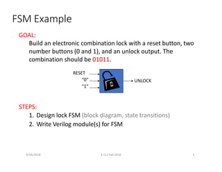
- 1. FSM Example GOAL: Build an electronic combination lock with a reset button, two number buttons (0 and 1), and an unlock output. The combination should be 01011. RESET ŌĆ£0ŌĆØ ŌĆ£1ŌĆØ 9/26/2018 6.111 Fall 2018 1 UNLOCK STEPS: 1. Design lock FSM (block diagram, state transitions) 2. Write Verilog module(s) for FSM
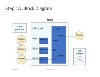
- 2. Step 1A: Block Diagram fsm_clock reset b0_in b1_in lock button button button Clock generator Button Reset Button 0 Button 1 fsm state unlock reset b0 b1 LED DISPLAY Unlock 9/26/2018 6.111 Fall 2018 2 LED
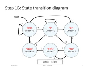
- 3. Step 1B: State transition diagram RESET Unlock = 0 ŌĆ£0ŌĆØ Unlock = 0 ŌĆ£01ŌĆØ Unlock = 0 ŌĆ£01011ŌĆØ Unlock = 1 ŌĆ£0101ŌĆØ Unlock = 0 ŌĆ£010ŌĆØ Unlock = 0 0 1 0 1 1 1 0 1 0 0 1 0 RESET 6 states ’é« 3 bits 9/26/2018 6.111 Fall 2018 3
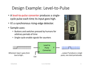
- 4. Design Example: LevelŌĆÉtoŌĆÉPulse ŌĆó A levelŌĆÉtoŌĆÉpulse converter produces a singleŌĆÉ cycle pulse each time its input goes high. ŌĆó ItŌĆÖs a synchronous risingŌĆÉedge detector. ŌĆó Sample uses: ŌĆó Buttons and switches pressed by humans for arbitrary periods of time ŌĆó SingleŌĆÉcycle enable signals for counters L Level to Pulse P Converter CLK Whenever input L goes from low to high... 9/26/2018 6.111 Fall 2018 4 ...output P produces a single pulse, one clock period wide.
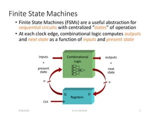
- 5. Finite State Machines ŌĆó Finite State Machines (FSMs) are a useful abstraction for sequential circuits with centralized ŌĆ£statesŌĆØ of operation ŌĆó At each clock edge, combinational logic computes outputs and next state as a function of inputs and present state Combinational Logic Registers Q D CLK inputs + present state outputs + next state n n 9/26/2018 6.111 Fall 2018 5
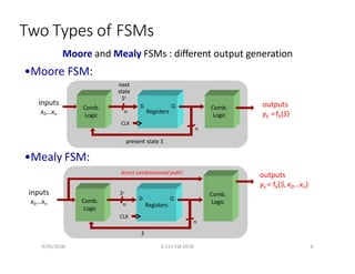
- 6. Two Types of FSMs outputs yk =fk(S) inputs x0...xn Comb. Logic CLK Registers Comb. Logic D Q n present state S n Moore and Mealy FSMs : different output generation ŌĆóMoore FSM: next state S+ inputs x0...xn ŌĆóMealy FSM: S Comb. Logic CLK Comb. Logic D Q Registers S+ n n outputs yk = fk(S,x0...xn) 9/26/2018 6.111 Fall 2018 6 direct combinational path!
- 7. Design Example: LevelŌĆÉtoŌĆÉPulse ŌĆó A levelŌĆÉtoŌĆÉpulse converter produces a singleŌĆÉ cycle pulse each time its input goes high. ŌĆó ItŌĆÖs a synchronous risingŌĆÉedge detector. ŌĆó Sample uses: ŌĆó Buttons and switches pressed by humans for arbitrary periods of time ŌĆó SingleŌĆÉcycle enable signals for counters L Level to Pulse P Converter CLK Whenever input L goes from low to high... 9/26/2018 6.111 Fall 2018 7 ...output P produces a single pulse, one clock period wide.
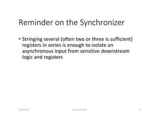
- 8. 9/26/2018 6.111 Fall 2018 8 Reminder on the Synchronizer ŌĆó Stringing several (often two or three is sufficient) registers in series is enough to isolate an asynchronous input from sensitive downstream logic and registers
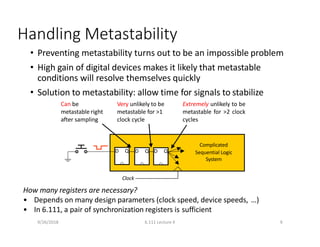
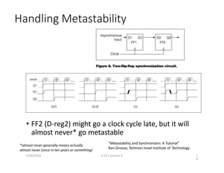
- 9. Handling Metastability ŌĆó Preventing metastability turns out to be an impossible problem ŌĆó High gain of digital devices makes it likely that metastable conditions will resolve themselves quickly ŌĆó Solution to metastability: allow time for signals to stabilize D Q Complicated Sequential Logic System Clock How many registers are necessary? ŌĆó Depends on many design parameters (clock speed, device speeds, ŌĆ”) ŌĆó In 6.111, a pair of synchronization registers is sufficient D Q D Q Can be metastable right after sampling Very unlikely to be metastable for >1 clock cycle Extremely unlikely to be metastable for >2 clock cycles 9/26/2018 6.111 Lecture 4 9
- 10. Handling Metastability ŌĆó FF2 (DŌĆÉreg2) might go a clock cycle late, but it will almost never* go metastable ŌĆ£Metastability and Synchronizers: A TutorialŌĆØ Ran Ginosar, Technion Israel Institute of Technology 9/26/2018 6.111 Lecture 4 1 0 *almost never generally means actually almost never (once in ten years or something)
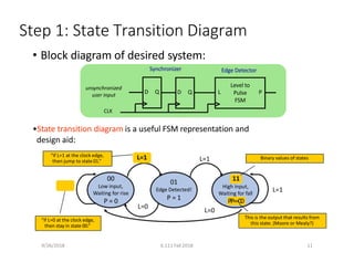
- 11. L=0 00 Low input, Waiting for rise P = 0 01 Edge Detected! P = 1 L=1 L=0 L=0 L=1 ŌĆóState transition diagram is a useful FSM representation and design aid: Step 1: State Transition Diagram ŌĆó Block diagram of desired system: D Q Level to Pulse FSM L P unsynchronized user input Synchronizer Edge Detector This is the output that results from this state. (Moore or Mealy?) 11 High input, Waiting for fall PP==00 Binary values of states ŌĆ£if L=0 at the clock edge, then stay in state 00.ŌĆØ L=1 ŌĆ£if L=1 at the clock edge, then jump to state 01.ŌĆØ D Q CLK 9/26/2018 6.111 Fall 2018 11
- 12. Valid State Transition Diagrams 11 High input, Waiting for fall P = 0 9/26/2018 6.111 Fall 2018 12 L=1 L=0 00 Low input, Waiting for rise P = 0 01 Edge Detected! P = 1 L=1 L=0 L=0 L=1 ŌĆó Arcs leaving a state are mutually exclusive, i.e., for any combination input values thereŌĆÖs at most one applicable arc ŌĆó Arcs leaving a state are collectively exhaustive, i.e., for any combination of input values thereŌĆÖs at least one applicable arc ŌĆó So for each state: for any combination of input values thereŌĆÖs exactly one applicable arc ŌĆó Often a starting state is specified ŌĆó Each state specifies values for all outputs (Moore)
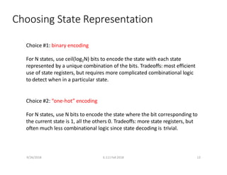
- 13. 9/26/2018 6.111 Fall 2018 13 Choosing State Representation Choice #1: binary encoding For N states, use ceil(log2N) bits to encode the state with each state represented by a unique combination of the bits. Tradeoffs: most efficient use of state registers, but requires more complicated combinational logic to detect when in a particular state. Choice #2: ŌĆ£oneŌĆÉhotŌĆØ encoding For N states, use N bits to encode the state where the bit corresponding to the current state is 1, all the others 0. Tradeoffs: more state registers, but often much less combinational logic since state decoding is trivial.
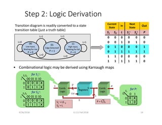
- 14. Step 2: Logic Derivation 00 Low input, Waiting for rise P = 0 01 Edge Detected! P = 1 L=0 11 High input, Waiting for fall P = 0 L=0 L=0 L=1 Current State In Next State Out S1 S0 L S + 1 S + 0 P 0 0 0 0 0 0 0 0 1 0 1 0 0 1 0 0 0 1 0 1 1 1 1 1 1 1 0 0 0 0 1 1 1 1 1 0 Transition diagram is readily converted to a state transition table (just a truth table) L=1 L=1 ŌĆó Combinational logic may be derived using Karnaugh maps 0 1 0 0 0 X 0 1 1 X 0 1 0 0 0 X 1 1 1 X S1S0 L 00 01 11 10 S1S0 L 00 01 11 10 1 for S +: 0 for S +: 0 1 0 X 1 0 S1 for P: 0 1 S0 Comb. Logic n Registers Comb. Logic D Q S n CLK S+ L P 1 S + =LS 0 0 S + =L P = S1S0 9/26/2018 6.111 Fall 2018 14
- 15. Moore LevelŌĆÉtoŌĆÉPulse Converter Moore FSM circuit implementation of levelŌĆÉtoŌĆÉpulse converter: outputs yk =fk(S) inputs x0...xn Comb. Logic CLK Registers Comb. Logic D Q n present state S n next state S+ D Q 1 S + =LS 0 0 S + =L P = S1S0 P = S1S0 S0 1 CLK 0 S + 1 S + L P Q D Q S Q 9/26/2018 6.111 Fall 2018 15
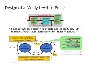
- 16. 1. When L=1 and S=0, this output is asserted immediately and until the state transition occurs (or L changes). 2. While in state S=1 and as long as L remains at 1, this output is asserted until next clock. L=1 | P=0 L=1 | P=1 0 Input is low 1 Input is high L=0 | P=0 L=0 | P=0 Design of a Mealy LevelŌĆÉtoŌĆÉPulse S ŌĆó Since outputs are determined by state and inputs, Mealy FSMs may need fewer states than Moore FSM implementations Comb. Logic Registers Comb. Logic D Q S+ n CLK n direct combinational path! L State P Clock Output transitions immediately. State transitions at the clock edge. 1 2 9/26/2018 6.111 Fall 2018 16
- 17. Mealy LevelŌĆÉtoŌĆÉPulse Converter Pres. State In Next State Out S L S+ P 0 0 0 1 0 1 0 1 1 1 1 0 1 0 0 0 D Q S CLK S+ Mealy FSM circuit implementation of levelŌĆÉtoŌĆÉpulse converter: P L Q S ŌĆó FSMŌĆÖs state simply remembers the previous value of L ŌĆó Circuit benefits from the Mealy FSMŌĆÖs implicit singleŌĆÉcycle assertion of outputs during state transitions 0 Input is low 9/26/2018 6.111 Fall 2018 17 1 Input is high L=1 | P=1 L=0 | P=0 L=1 | P=0 L=0 | P=0
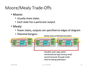
- 18. Moore/Mealy TradeŌĆÉOffs ŌĆó How are they different? ŌĆó Moore: outputs = f( state ) only ŌĆó Mealy outputs = f( state and input ) ŌĆó Mealy outputs generally occur one cycle earlier than a Moore: Moore: delayed assertion of P Mealy: immediate assertion of P L L P P Clock Clock State[0] State ŌĆó Compared to a Moore FSM, a Mealy FSM might... ŌĆō Be more difficult to conceptualize and design ŌĆō Have fewer states 9/26/2018 6.111 Fall 2018 18
- 19. ŌĆó Moore: ŌĆó Usually more states ŌĆó Each state has a particular output ŌĆó Mealy: ŌĆó Fewer states, outputs are specified on edges of diagram ŌĆó Potential Dangers: Moore/Mealy TradeŌĆÉOffs ReallyŌĆÉlong combinatorial paths! Possible cyclic logic paths Combinatorial logic driving itself asynchronously through really hardŌĆÉtoŌĆÉdebug pathways! 9/26/2018 6.111 Fall 2018 19
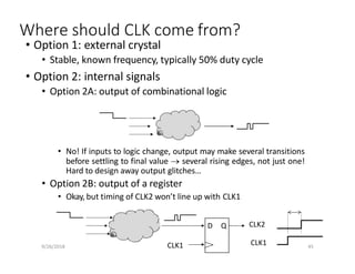
- 20. 9/26/2018 45 Where should CLK come from? ŌĆó Option 1: external crystal ŌĆó Stable, known frequency, typically 50% duty cycle ŌĆó Option 2: internal signals ŌĆó Option 2A: output of combinational logic ŌĆó No! If inputs to logic change, output may make several transitions before settling to final value ’é« several rising edges, not just one! Hard to design away output glitchesŌĆ” ŌĆó Option 2B: output of a register ŌĆó Okay, but timing of CLK2 wonŌĆÖt line up with CLK1 D Q CLK1 CLK2 CLK1
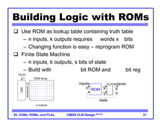
- 21. CMOS VLSI Design CMOS VLSI Design 4th Ed. 20: CAMs, ROMs, and PLAs 21 Building Logic with ROMs ’ü▒ Use ROM as lookup table containing truth table ŌĆō n inputs, k outputs requires 2n words x k bits ŌĆō Changing function is easy ŌĆō reprogram ROM ’ü▒ Finite State Machine ŌĆō n inputs, k outputs, s bits of state ŌĆō Build with 2n+s x (k+s) bit ROM and (k+s) bit reg n inputs 2 n wordlines ROM Array k outputs DEC ROM inputs outputs state n k s k s
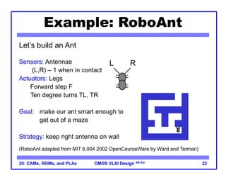
- 22. CMOS VLSI Design CMOS VLSI Design 4th Ed. 20: CAMs, ROMs, and PLAs 22 Example: RoboAnt LetŌĆÖs build an Ant Sensors: Antennae (L,R) ŌĆō 1 when in contact Actuators: Legs Forward step F Ten degree turns TL, TR Goal: make our ant smart enough to get out of a maze Strategy: keep right antenna on wall (RoboAnt adapted from MIT 6.004 2002 OpenCourseWare by Ward and Terman) L R
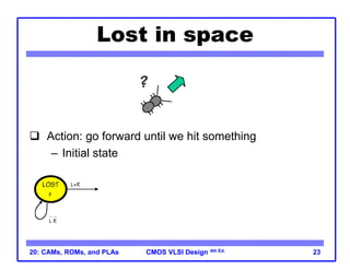
- 23. CMOS VLSI Design CMOS VLSI Design 4th Ed. 20: CAMs, ROMs, and PLAs 23 Lost in space ’ü▒ Action: go forward until we hit something ŌĆō Initial state
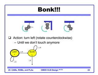
- 24. CMOS VLSI Design CMOS VLSI Design 4th Ed. 20: CAMs, ROMs, and PLAs 24 Bonk!!! ’ü▒ Action: turn left (rotate counterclockwise) ŌĆō Until we donŌĆÖt touch anymore
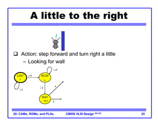
- 25. CMOS VLSI Design CMOS VLSI Design 4th Ed. 20: CAMs, ROMs, and PLAs 25 A little to the right ’ü▒ Action: step forward and turn right a little ŌĆō Looking for wall
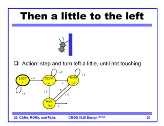
- 26. CMOS VLSI Design CMOS VLSI Design 4th Ed. 20: CAMs, ROMs, and PLAs 26 Then a little to the left ’ü▒ Action: step and turn left a little, until not touching
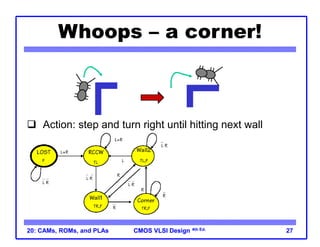
- 27. CMOS VLSI Design CMOS VLSI Design 4th Ed. 20: CAMs, ROMs, and PLAs 27 Whoops ŌĆō a corner! ’ü▒ Action: step and turn right until hitting next wall
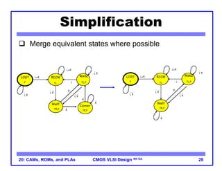
- 28. CMOS VLSI Design CMOS VLSI Design 4th Ed. 20: CAMs, ROMs, and PLAs 28 Simplification ’ü▒ Merge equivalent states where possible
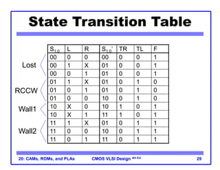
- 29. CMOS VLSI Design CMOS VLSI Design 4th Ed. 20: CAMs, ROMs, and PLAs 29 State Transition Table S1:0 L R S1:0ŌĆÖ TR TL F 00 0 0 00 0 0 1 00 1 X 01 0 0 1 00 0 1 01 0 0 1 01 1 X 01 0 1 0 01 0 1 01 0 1 0 01 0 0 10 0 1 0 10 X 0 10 1 0 1 10 X 1 11 1 0 1 11 1 X 01 0 1 1 11 0 0 10 0 1 1 11 0 1 11 0 1 1 Lost RCCW Wall1 Wall2
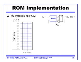
- 30. CMOS VLSI Design CMOS VLSI Design 4th Ed. 20: CAMs, ROMs, and PLAs 30 ROM Implementation ’ü▒ 16-word x 5 bit ROM ROM L, R S1:0 TL, TR, F S'1:0 S1 ' S0 ' TR'TL' F' 0000 0001 0010 0011 0100 0101 0110 0111 1000 1001 1010 1011 1100 1101 1110 1111 4:16 DEC S1 S0 L R
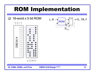
- 31. CMOS VLSI Design CMOS VLSI Design 4th Ed. 20: CAMs, ROMs, and PLAs 31 ROM Implementation ’ü▒ 16-word x 5 bit ROM ROM L, R S1:0 TL, TR, F S'1:0 S1 ' S0 ' TR'TL' F' 0000 0001 0010 0011 0100 0101 0110 0111 1000 1001 1010 1011 1100 1101 1110 1111 4:16 DEC S1 S0 L R