ResearchProject2009
1 like257 views

Ibrahim Hazmi presents work on redesigning the CPU12 microcontroller using VHDL. The document outlines a methodology for partitioning the design into blocks and describes work done on the register block, ALU, control unit, and simulations. Future work includes finishing the control unit, connecting it to the data path, and designing the pre-fetch unit. The goal is to gain understanding of embedded system design and combine that with HDL skills.
![Wednesday 01/07/2009IBRAHIM HAZMI - SECE
[D, IDX] - Indexed-indirect; Acc D offset (1011)
32](https://image.slidesharecdn.com/12099f27-b4cc-4052-a280-e21eb4ed7eb4-151027005351-lva1-app6891/85/ResearchProject2009-32-320.jpg)
![Wednesday 01/07/2009IBRAHIM HAZMI - SECE
[IDX2]âIDX-IND; 16-bit (1010)
33](https://image.slidesharecdn.com/12099f27-b4cc-4052-a280-e21eb4ed7eb4-151027005351-lva1-app6891/85/ResearchProject2009-33-320.jpg)
ResearchProject2009
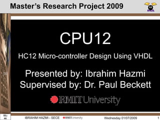
- 1. Wednesday 01/07/2009IBRAHIM HAZMI - SECE Masterâs Research Project 2009 1 CONTROL UNIT ADRESS CAL-CIRCUIT REG BLOCK ALU Pre-Fetch UNIT Memory Access Unit CPU12 Presented by: Ibrahim Hazmi Supervised by: Dr. Paul Beckett HC12 Micro-controller Design Using VHDL
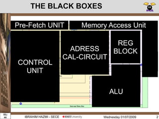
- 2. Wednesday 01/07/2009IBRAHIM HAZMI - SECE THE BLACK BOXES 2 CONTROL UNIT ADRESS CAL-CIRCUIT REG BLOCK ALU Pre-Fetch UNIT Memory Access Unit
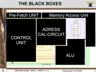
- 3. Wednesday 01/07/2009IBRAHIM HAZMI - SECE THE BLACK BOXES 3 CONTROL UNIT ADRESS CAL-CIRCUIT ALU Pre-Fetch UNIT Memory Access Unit
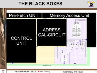
- 4. Wednesday 01/07/2009IBRAHIM HAZMI - SECE THE BLACK BOXES 4 CONTROL UNIT ADRESS CAL-CIRCUIT Pre-Fetch UNIT Memory Access Unit
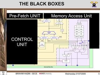
- 5. Wednesday 01/07/2009IBRAHIM HAZMI - SECE THE BLACK BOXES 5 CONTROL UNIT Pre-Fetch UNIT Memory Access Unit
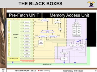
- 6. Wednesday 01/07/2009IBRAHIM HAZMI - SECE THE BLACK BOXES 6 Pre-Fetch UNIT Memory Access Unit
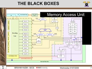
- 7. Wednesday 01/07/2009IBRAHIM HAZMI - SECE THE BLACK BOXES 7 Memory Access Unit
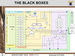
- 8. Wednesday 01/07/2009IBRAHIM HAZMI - SECE THE BLACK BOXES 8
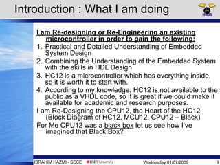
- 9. Wednesday 01/07/2009IBRAHIM HAZMI - SECE Introduction : What I am doing I am Re-designing or Re-Engineering an existing microcontroller in order to gain the following: 1. Practical and Detailed Understanding of Embedded System Design 2. Combining the Understanding of the Embedded System with the skills in HDL Design 3. HC12 is a microcontroller which has everything inside, so it is worth it to start with. 4. According to my knowledge, HC12 is not available to the public as a VHDL code, so it is great if we could make it available for academic and research purposes. I am Re-Designing the CPU12, the Heart of the HC12 (Block Diagram of HC12, MCU12, CPU12 â Black) For Me CPU12 was a black box let us see how Iâve imagined that Black Box? 9
- 10. Wednesday 01/07/2009 10IBRAHIM HAZMI - SECE âĒ AT the Beginning, I was taking every part of Micro as a separate part and design it without any guidelines except its functionality, which was bringing difficulty to join all parts together at the end. Also it was leading me to put unnecessary circuits into it. âĒ In this project, Iâve learnt a good methodology in designing a microprocessor: âĒ I need to thank Two Ideas in this regard: Methodology Wednesday 01/07/2009
- 11. Wednesday 01/07/2009 11IBRAHIM HAZMI - SECE âĒ 1st: âIn designing a CPU, we must first define its instruction set, and how the instructions are encoded and executed. We need to answer questions such as how many instructions do we want? What are the instructions? What operation code (opcode) do we assign to each of the instructions? How many bits do we use to encode an instruction? Once we have decided on the instruction set, we can proceed to designing a datapath that can execute all the instructions in the instruction set. In this step we are creating a custom datapath, so we need to answer questions such as what functional units do we need? How many registers do we need? Do we use a single register file or separate registers? How are the different units connected together?â Enoch O. Hwang, 2005, Digital Logic and Microprocessor Design With VHDL, La Sierra University, Riverside This Quote was my leader to understand how to start when designing a microprocessor. Dr Hwang From in USA Methodology
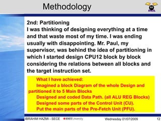
- 12. Wednesday 01/07/2009IBRAHIM HAZMI - SECE 2nd: Partitioning I was thinking of designing everything at a time and that waste most of my time. I was ending usually with disappointing. Mr. Paul, my supervisor, was behind the idea of partitioning in which I started design CPU12 block by block considering the relations between all blocks and the target instruction set. Methodology 12 What I have achieved: Imagined a block Diagram of the whole Design and partitioned it to 5 Main Blocks Designed and coded Data Path. (all ALU REG Blocks) Designed some parts of the Control Unit (CU). Put the main parts of the Pre-Fetch Unit (PFU).
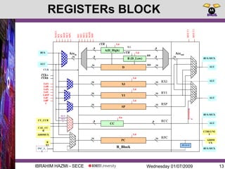
- 13. Wednesday 01/07/2009IBRAHIM HAZMI - SECE REGISTERs BLOCK 13 R_Block CLK Accin Accout A(D_High) D B (D_Low) XI CC 16 RA RB RCC RSP RXI RYI RPC 8 8 RD 8 8 16 16 16 88 1616 YI 1616 SP 1616 PC 1616 CLR CLR Ld Ld Ld Ld Ld Ld En A L U B A L U A ALU BUS CAL_CC R CU_CCR R EL ALU BUS-MUX PC+1/+2 ADDMUX ALU CLRA CLRB LdA LdB LdX LdY LdSP LdC CLdP C MACC MX MY MSP MCC MPC MOUT1 MOUT2 00000000C C BUS LALU L ALU BUS-MUX CTRLUNI T ADDM UX BUS-MUX ALU MI1 MI2 MO1 MO2 MAB M0F INC_1_ 2
- 14. Wednesday 01/07/2009IBRAHIM HAZMI - SECE REGISTERs BLOCK 14 D A B MUXAcc BUSALU RMUX1 RMU X2
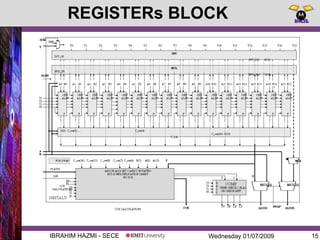
- 15. Wednesday 01/07/2009IBRAHIM HAZMI - SECE REGISTERs BLOCK 15
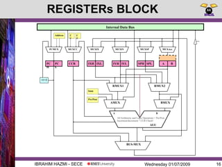
- 16. Wednesday 01/07/2009IBRAHIM HAZMI - SECE REGISTERs BLOCK 16 IXH IXL IYH IYL SPH SPL Internal Data Bus CCR BMUX A B BA ALU All Arithmetic and Logic Operations + Pre/Post Increment/decrement + CCR Check! RMUX2RMUX1 BUS-MUX PC H PC L PCMUX +1/+2 MUXIX MUXSPMUXIY MUXAcc AMUX MUXCC Pre/Post Imm Address C C C U
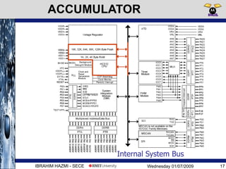
- 17. Wednesday 01/07/2009IBRAHIM HAZMI - SECE ACCUMULATOR 17 Internal System Bus
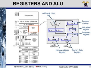
- 18. Wednesday 01/07/2009IBRAHIM HAZMI - SECE REGISTERS AND ALU 18 ALU A B D MAR MDR PC IR 1 6 1 6 ADDR15:0 DATA15:0 T Program Counter Instruction Register Memory Data Register Memory Address Register Arithmetic Logic Unit Temporary Register
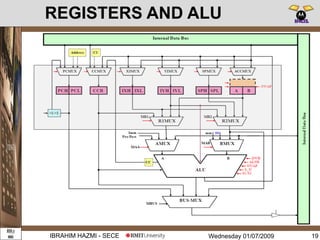
- 19. Wednesday 01/07/2009IBRAHIM HAZMI - SECE REGISTERS AND ALU 19
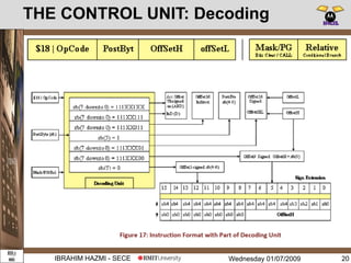
- 20. Wednesday 01/07/2009IBRAHIM HAZMI - SECE THE CONTROL UNIT: Decoding 20
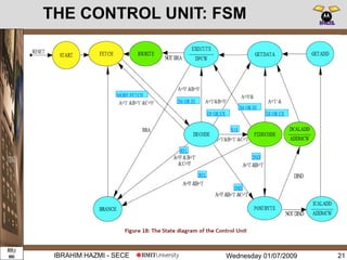
- 21. Wednesday 01/07/2009IBRAHIM HAZMI - SECE THE CONTROL UNIT: FSM 21
- 22. Wednesday 01/07/2009IBRAHIM HAZMI - SECE SIMULATIONS 22
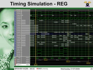
- 23. Wednesday 01/07/2009IBRAHIM HAZMI - SECE Timing Simulation - REG 23
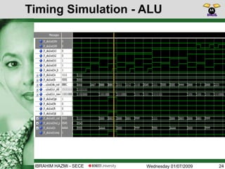
- 24. Wednesday 01/07/2009IBRAHIM HAZMI - SECE Timing Simulation - ALU 24
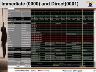
- 25. Wednesday 01/07/2009IBRAHIM HAZMI - SECE Immediate (0000) and Direct(0001) 25
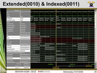
- 26. Wednesday 01/07/2009IBRAHIM HAZMI - SECE Extended(0010) & Indexed(0011) 26
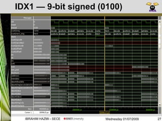
- 27. Wednesday 01/07/2009IBRAHIM HAZMI - SECE IDX1 â 9-bit signed (0100) 27
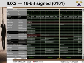
- 28. Wednesday 01/07/2009IBRAHIM HAZMI - SECE IDX2 â 16-bit signed (0101) 28
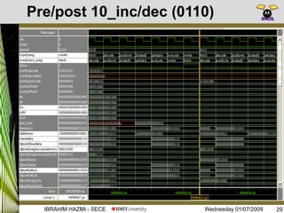
- 29. Wednesday 01/07/2009IBRAHIM HAZMI - SECE Pre/post 10_inc/dec (0110) 29
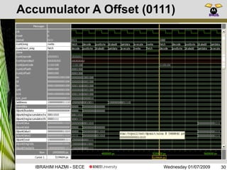
- 30. Wednesday 01/07/2009IBRAHIM HAZMI - SECE Accumulator A Offset (0111) 30
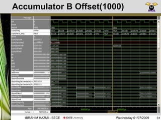
- 31. Wednesday 01/07/2009IBRAHIM HAZMI - SECE Accumulator B Offset(1000) 31
- 32. Wednesday 01/07/2009IBRAHIM HAZMI - SECE [D, IDX] - Indexed-indirect; Acc D offset (1011) 32
- 33. Wednesday 01/07/2009IBRAHIM HAZMI - SECE [IDX2]âIDX-IND; 16-bit (1010) 33
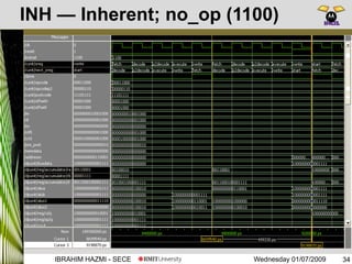
- 34. Wednesday 01/07/2009IBRAHIM HAZMI - SECE INH â Inherent; no_op (1100) 34
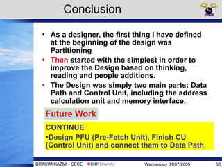
- 35. Wednesday 01/07/2009IBRAHIM HAZMI - SECE Conclusion âĒ As a designer, the first thing I have defined at the beginning of the design was Partitioning âĒ Then started with the simplest in order to improve the Design based on thinking, reading and people additions. âĒ The Design was simply two main parts: Data Path and Control Unit, including the address calculation unit and memory interface. 35 CONTINUE âĒDesign PFU (Pre-Fetch Unit), Finish CU (Control Unit) and connect them to Data Path. Future Work
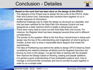
- 36. Wednesday 01/07/2009IBRAHIM HAZMI - SECE Conclusion - Detailes Based on the work that has been done on the design of the CPU12: The objective of the Project was to design the two units of the CPU12, (Data Path and Control Unit), individually then combine them together to run a simple sequence of instructions. Additional challenge was to make the design as structural as it possible, and that has been satisïŽed for the Data Path Unit whereas Control unit was designed as a state machine which is totally in behavioural Level. There were many trials to come out with ïŽnal Data Path Unit circuits. For instance, the Register block has been designed several times and in different considerations. The answer to the question: What is the ïŽrst thing I should know in doing such design was the key of the understanding and imagination of what id going on. It leads, at then end, to draw a reasonable block diagram that meets the requirements. The Idea of Partitioning was behind the ability to design CPU12 block by block considering the relations between all blocks and the targeted instruction set. During my work in this design, Iâve got the Idea of starting with the simplest then improve the Design based on thinking, reading and people additions. Iâve gained a good understanding of how embedded systems work, how to manage a microcontroller processes and how to connect its parts together in order to run a simple code. 36
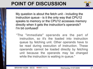
- 37. Wednesday 01/07/2009 37IBRAHIM HAZMI - SECE âThe "immediate" operands are the part of instruction, so it's the loaded into instruction queue by fetching unit. Other operands have to be read during execution of instruction. These operands cannot be loaded directly by fetching unit because the operands may be changed while the instruction is waiting in queue.â POINT OF DISCUSSION My question is about the fetch unit - including the Instruction queue - is it the only way that CPU12 speaks to memory or the CPU12 accesses memory directly when it gets the instruction's operands? I'm bit confused!
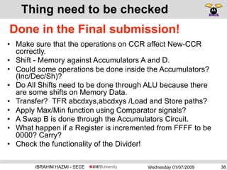
- 38. Wednesday 01/07/2009IBRAHIM HAZMI - SECE Thing need to be checked âĒ Make sure that the operations on CCR affect New-CCR correctly. âĒ Shift - Memory against Accumulators A and D. âĒ Could some operations be done inside the Accumulators? (Inc/Dec/Sh)? âĒ Do All Shifts need to be done through ALU because there are some shifts on Memory Data. âĒ Transfer? TFR abcdxys,abcdxys /Load and Store paths? âĒ Apply Max/Min function using Comparator signals? âĒ A Swap B is done through the Accumulators Circuit. âĒ What happen if a Register is incremented from FFFF to be 0000? Carry? âĒ Check the functionality of the Divider! 38 Done in the Final submission!
- 39. Wednesday 01/07/2009IBRAHIM HAZMI - SECE References 1. Enoch O. Hwang, 2005, Digital Logic and Microprocessor Design With VHDL, La Sierra University, Riverside, USA. 2. Altera Co, 2009, AN 311: Standard Cell ASIC to FPGA Design, Methodology and Guidelines 3. E. OstÚa, J. Juan Chico, J. Viejo, M. J. Bellido, D. Guerrero, A. MillÃĄn & P. Ruiz-de-Clavijo, AN SOC DESIGN METHODOLOGY FOR LEON2 ON FPGA, Universidad de Sevilla. 4. Volnei A. Pedroni, 2004, Circuit Design with VHDL, MIT Press, Cambridge, Massachusetts, London, England 5. PONG P. CHU, 2006, RTL HARDWARE DESIGN USING VHDL, Cleveland State University, WlLEY INTERSCIENCE. 6. Peter J. Ashenden, 1990, The VHDL Cookbook, Dept. Computer Science, University of Adelaide, SA, 1ST Edition 7. M. Morris Mano, 1993, Computer System Architecture, 3rd Edition, Prentice Hall Int. 8. Digitaaltehnika erikursus, Digital Design Methodology 9. Freescale Semiconductor, 2006, CPU12 Reference Manual (CPU12RM); Motorola M68HC12 and HCS12 Microcontrollers, Rev. 4.0 10. HC11: http://online.sfsu.edu/~valverde/ENGR/ENGR478_s07/welcome.htm, Dr. Ricardo V., 2004, Lecture Notes; ENGR 478, 11. LC3: http://www.et.byu.edu/groups/ece224web/lectures/LC3-2.pdf, 20/07/2009 12. http://www.eng.auburn.edu/~nelson/, 13/03/2009. 13. http://oucsace.cs.ohiou.edu/~avinashk/, 13/03/2009. 14. http://cs.lasierra.edu/~ehwang/mybook/toc.html, 13/03/2009. 15. http://lap2.epïŽ.ch/courses/archord1/, 13/03/2009. 16. http://www.ece.tamu.edu/~vinith/ecen248/index_ïŽles/lab_manual_spring09.pdf, 13/03/2009 17. http://www.eda-stds.org/rassp/, 13/03/2009. 18. http://vlsi.ee.hacettepe.edu.tr/links.html, 13/03/2009. 19. Reto Z., 1999, Lecture notes on Computer Arithmetic: Principles, Architectures, and VLSI Design, Integrated Systems Laboratory, Swiss Federal Institute of Technology (ETH), Switzerland. 39
- 40. Wednesday 01/07/2009IBRAHIM HAZMI - SECE THANK YOU 40