
![Fetching a Word from Memory
’ü¼ The response time of each memory access varies
(cache miss, memory-mapped I/O,ŌĆ”).
’ü¼ To accommodate this, the processor waits until it
receives an indication that the requested operation
has been completed (Memory-Function-Completed,
MFC).
’ü¼ Move (R1), R2
’āś MAR ŌåÉ [R1]
’āś Start a Read operation on the memory bus
’āś Wait for the MFC response from the memory
’āś Load MDR from the memory bus
’āś R2 ŌåÉ [MDR]](https://image.slidesharecdn.com/unit-3processororganization-240806102731-eff5d8ca/85/UNIT-3-Processor-Organization-_computer-organization-ppt-8-320.jpg)
![Timing
Figure 7.5. Timing of a memory Read operation.
1 2
Clock
Address
MR
Data
MFC
Read
MDRinE
MDRout
Step 3
MARin
Assume MAR
is always available
on the address lines
of the memory bus.
R2 ŌåÉ [MDR]
MAR ŌåÉ [R1]
Start a Read operation on the memory bus
Wait for the MFC response from the memory
Load MDR from the memory bus](https://image.slidesharecdn.com/unit-3processororganization-240806102731-eff5d8ca/85/UNIT-3-Processor-Organization-_computer-organization-ppt-9-320.jpg)


![OP code 0 1 0 Rsrc Rdst
Mode
Contents of IR
0
3
4
7
8
10
11
Figure 7.21. Microinstruction for Add (Rsrc)+,Rdst.
Note: Microinstruction at location 170 is not executed for this addressing mode.
Address Microinstruction
(octal)
000 PCout, MARin , Read, Select
4 , Add, Zin
001 Zout, PCin, Yin, WMFC
002 MDRout, IRin
003 ’üŁBranch {
’üŁ PC’é¼ 101 (from Instruction decoder);
’üŁPC5,4 ’é¼ [IR10,9]; ’üŁPC3 ’é¼
121 Rsrcout, MARin , Read, Select4, Add, Z
in
122 Zout , Rsrcin
123
170 MDRout, MARin , Read, WMFC
171 MDRout, Yin
172 Rdstout , SelectY
, Add, Zin
173 Zout , Rdstin, End
[IR10]’āŚ[IR9]’āŚ[IR8]}
’üŁBranch {’üŁPC’é¼ 170;’üŁPC0 ’é¼ [IR8]}, WMFC](https://image.slidesharecdn.com/unit-3processororganization-240806102731-eff5d8ca/85/UNIT-3-Processor-Organization-_computer-organization-ppt-37-320.jpg)

UNIT-3(Processor Organization)_computer organization.ppt
- 2. Fundamental Concepts ’ü¼ Processor fetches one instruction at a time and perform the operation specified. ’ü¼ Instructions are fetched from successive memory locations until a branch or a jump instruction is encountered. ’ü¼ Processor keeps track of the address of the memory location containing the next instruction to be fetched using Program Counter (PC). ’ü¼ Instruction Register (IR)
- 3. Executing an Instruction ’ü¼ Transfer a word of data from one processor register to another or to the ALU. ’ü¼ Perform an arithmetic or a logic operation and store the result in a processor register. ’ü¼ Fetch the contents of a given memory location and load them into a processor register. ’ü¼ Store a word of data from a processor register into a given memory location.
- 4. Register Transfers B A Z ALU Yin Y Zin Zout Riin Ri Riout bus Internal processor Constant 4 MUX Figure 7.2. Input and output gating for the registers in Figure 7.1. Select
- 5. Register Transfers ’ü¼ All operations and data transfers are controlled by the processor clock. Figure 7.3. Input and output gating for one register bit. D Q Q Clock 1 0 Riout Riin Bus Figure 7.3. Input and output gating for one register bit.
- 6. Performing an Arithmetic or Logic Operation ’ü¼ The ALU is a combinational circuit that has no internal storage. ’ü¼ ALU gets the two operands from MUX and bus. The result is temporarily stored in register Z. ’ü¼ What is the sequence of operations to add the contents of register R1 to those of R2 and store the result in R3? 1. R1out, Yin 2. R2out, SelectY, Add, Zin 3. Zout, R3in
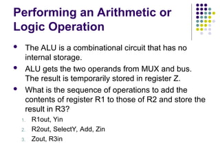
- 7. Fetching a Word from Memory ’ü¼ Address into MAR; issue Read operation; data into MDR. MDR Memory-bus Figure 7.4. Connection and control signals for register MDR. data lines Internal processor bus MDRout MDRoutE MDRin MDRinE Figure 7.4. Connection and control signals for register MDR.
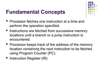
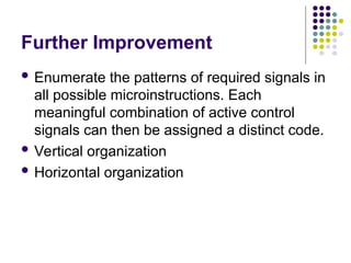
- 8. Fetching a Word from Memory ’ü¼ The response time of each memory access varies (cache miss, memory-mapped I/O,ŌĆ”). ’ü¼ To accommodate this, the processor waits until it receives an indication that the requested operation has been completed (Memory-Function-Completed, MFC). ’ü¼ Move (R1), R2 ’āś MAR ŌåÉ [R1] ’āś Start a Read operation on the memory bus ’āś Wait for the MFC response from the memory ’āś Load MDR from the memory bus ’āś R2 ŌåÉ [MDR]
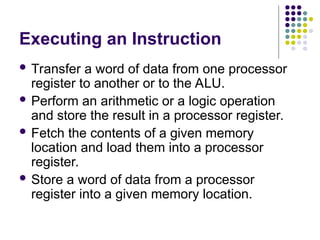
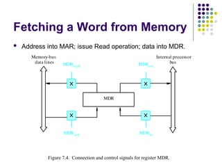
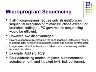
- 9. Timing Figure 7.5. Timing of a memory Read operation. 1 2 Clock Address MR Data MFC Read MDRinE MDRout Step 3 MARin Assume MAR is always available on the address lines of the memory bus. R2 ŌåÉ [MDR] MAR ŌåÉ [R1] Start a Read operation on the memory bus Wait for the MFC response from the memory Load MDR from the memory bus
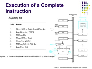
- 10. Execution of a Complete Instruction ’ü¼ Add (R3), R1 ’ü¼ Fetch the instruction ’ü¼ Fetch the first operand (the contents of the memory location pointed to by R3) ’ü¼ Perform the addition ’ü¼ Load the result into R1
- 11. Architecture B A Z ALU Yin Y Zin Zout Riin Ri Riout bus Internal processor Constant 4 MUX Figure 7.2. Input and output gating for the registers in Figure 7.1. Select
- 12. Execution of a Complete Instruction Step Action 1 PC out , MAR in , Read, Select4,Add, Zin 2 Zout , PC in , Yin , WMF C 3 MDR out , IR in 4 R3out , MAR in , Read 5 R1out , Yin , WMF C 6 MDR out , SelectY, Add, Zin 7 Zout , R1in , End Figure7.6. Control sequence for executionof theinstructionAdd (R3),R1. lines Data Address lines bus Memory Carry-in ALU PC MAR MDR Y Z Add XOR Sub bus IR TEMP R0 control ALU lines Control signals R n 1 - ’Ć© ’Ć® Instruction decoder and Internal processor control logic A B Figure 7.1. Single-bus organization of the datapath inside a processor. MUX Select Constant 4 Add (R3), R1
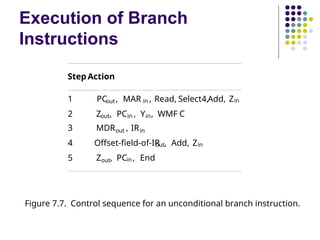
- 13. Execution of Branch Instructions ’ü¼ A branch instruction replaces the contents of PC with the branch target address, which is usually obtained by adding an offset X given in the branch instruction. ’ü¼ The offset X is usually the difference between the branch target address and the address immediately following the branch instruction. ’ü¼ Conditional branch
- 14. Execution of Branch Instructions Step Action 1 PCout, MAR in , Read, Select4,Add, Zin 2 Zout, PCin , Yin, WMF C 3 MDRout , IRin 4 Offset-field-of-IR out, Add, Zin 5 Zout, PCin , End Figure 7.7. Control sequence for an unconditional branch instruction.
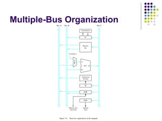
- 15. Multiple-Bus Organization Memory bus data lines Figure 7.8. Three-bus organization of the datapath. Bus A Bus B Bus C Instruction decoder PC Register file Constant 4 ALU MDR A B R MUX Incrementer Address lines MAR IR
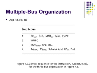
- 16. Multiple-Bus Organization ’ü¼ Add R4, R5, R6 Step Action 1 PCout, R=B, MAR in, Read, IncPC 2 WMFC 3 MDRoutB, R=B, IRin 4 R4outA, R5outB, SelectA, Add, R6in, End Figure 7.9.Control sequence for the instruction. Add R4,R5,R6, for the three-bus organization in Figure 7.8.
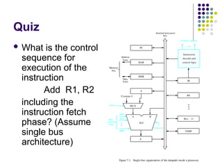
- 17. Quiz ’ü¼ What is the control sequence for execution of the instruction Add R1, R2 including the instruction fetch phase? (Assume single bus architecture) lines Data Address lines bus Memory Carry-in ALU PC MAR MDR Y Z Add XOR Sub bus IR TEMP R0 control ALU lines Control signals R n 1 - ’Ć© ’Ć® Instruction decoder and Internal processor control logic A B Figure 7.1. Single-bus organization of the datapath inside a processor. MUX Select Constant 4
- 19. Overview ’ü¼ To execute instructions, the processor must have some means of generating the control signals needed in the proper sequence. ’ü¼ Two categories: hardwired control and microprogrammed control ’ü¼ Hardwired system can operate at high speed; but with little flexibility.
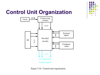
- 20. Control Unit Organization Figure 7.10. Control unit organization. CLK Clock Control step IR encoder Decoder/ Control signals codes counter inputs Condition External
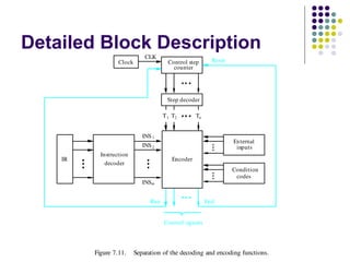
- 21. Detailed Block Description External inputs Figure 7.11. Separation of the decoding and encoding functions. Encoder Reset CLK Clock Control signals counter Run End Condition codes decoder Instruction Step decoder Control step IR T1 T2 Tn INS1 INS2 INSm
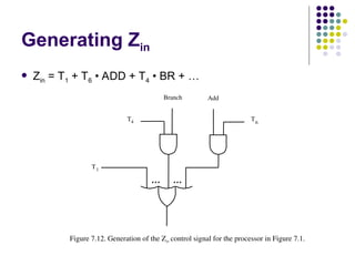
- 22. Generating Zin ’ü¼ Zin = T1 + T6 ŌĆó ADD + T4 ŌĆó BR + ŌĆ” Figure 7.12. Generation of the Zin control signal for the processor in Figure 7.1. T1 Add Branch T4 T6
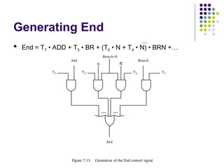
- 23. Generating End ’ü¼ End = T7 ŌĆó ADD + T5 ŌĆó BR + (T5 ŌĆó N + T4 ŌĆó N) ŌĆó BRN +ŌĆ” Figure 7.13. Generation of the End control signal. T7 Add Branch Branch<0 T5 End N N T4 T5
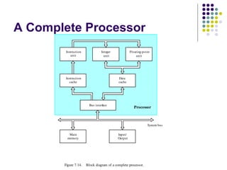
- 24. A Complete Processor Instruction unit Integer unit Floating-point unit Instruction cache Data cache Bus interf ace Main memory Input/ Output System bus Processor Figure 7.14. Block diagram of a complete processor.
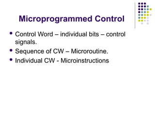
- 26. Microprogrammed Control ’ü¼ Control Word ŌĆō individual bits ŌĆō control signals. ’ü¼ Sequence of CW ŌĆō Microroutine. ’ü¼ Individual CW - Microinstructions
- 27. Overview ’ü¼ Control signals are generated by a program similar to machine language programs. ’ü¼ Control Word (CW); microroutine; microinstruction PC in PC out MAR in Read MDR out IR in Y in Select Add Z in Z out R1 out R1 in R3 out WMFC End 0 1 0 0 0 0 0 0 0 0 0 0 0 1 1 0 0 0 0 0 0 1 0 0 1 0 0 0 1 0 0 1 0 0 0 0 0 1 0 0 1 0 0 0 1 0 0 0 0 0 1 0 0 1 0 0 1 0 0 0 0 0 0 1 0 0 0 0 1 0 1 0 0 0 0 1 0 0 1 0 0 0 0 1 0 0 0 0 1 0 0 0 0 0 0 0 0 1 0 0 0 1 0 0 0 0 1 0 0 1 0 0 Micro - instruction 1 2 3 4 5 6 7 Figure 7.15 An example of microinstructions for Figure 7.6.
- 28. Overview Step Action 1 PC out , MAR in , Read, Select4,Add, Zin 2 Zout , PC in , Yin , WMF C 3 MDR out , IR in 4 R3out , MAR in , Read 5 R1out , Yin , WMF C 6 MDR out , SelectY, Add, Zin 7 Zout , R1in , End Figure7.6. Control sequence for executionof theinstructionAdd (R3),R1.
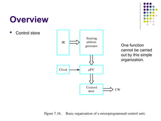
- 29. Overview ’ü¼ Control store Figure 7.16. Basic organization of a microprogrammed control unit. store Control generator Starting address CW Clock ’üŁPC IR One function cannot be carried out by this simple organization.
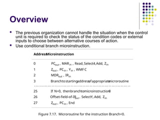
- 30. Overview ’ü¼ The previous organization cannot handle the situation when the control unit is required to check the status of the condition codes or external inputs to choose between alternative courses of action. ’ü¼ Use conditional branch microinstruction. Address Microinstruction 0 PCout , MARin , Read,Select4,Add, Zin 1 Zout , PCin , Yin , WMF C 2 MDRout , IRin 3 Branchtostartingaddress ofappropriate microroutine . ... .. ... ... .. ... .. ... ... .. ... ... .. ... .. ... ... .. ... .. ... ... .. ... .. 25 If N=0, thenbranchtomicroinstruction 0 26 Offset-field-of-IR out , SelectY, Add, Zin 27 Zout , PCin , End Figure 7.17. Microroutine for the instruction Branch<0.
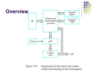
- 31. Overview Figure 7.18. Organization of the control unit to allow conditional branching in the microprogram. Control store Clock generator Starting and branch address Condition codes inputs External CW IR ’üŁPC
- 32. Microinstructions ’ü¼ A straightforward way to structure microinstructions is to assign one bit position to each control signal. ’ü¼ However, this is very inefficient. ’ü¼ The length can be reduced: most signals are not needed simultaneously, and many signals are mutually exclusive. ’ü¼ All mutually exclusive signals are placed in the same group in binary coding.
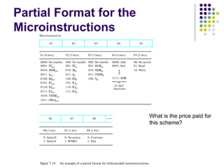
- 33. Partial Format for the Microinstructions F2 (3 bits) 000: No transfer 001: PC in 010: IR in 011: Zin 100: R0in 101: R1in 110: R2in 111: R3in F1 F2 F3 F4 F5 F1 (4 bits) F3 (3 bits) F4 (4 bits) F5 (2 bits) 0000: No transfer 0001: PC out 0010: MDR out 0011: Z out 0100: R0 out 0101: R1 out 0110: R2 out 0111: R3 out 1010: TEMP out 1011: Offsetout 000: No transfer 001: MARin 010: MDRin 011: TEMP in 100: Yin 0000: Add 0001: Sub 1111: XOR 16 ALU functions 00: No action 01: Read 10: Write F6 F7 F8 F6 (1 bit) F7 (1 bit) F8 (1 bit) 0: SelectY 1: Select4 0: No action 1: WMFC 0: Continue 1: End Figure 7.19. An example of a partial format for field-encoded microinstructions. Microinstruction What is the price paid for this scheme?
- 34. Further Improvement ’ü¼ Enumerate the patterns of required signals in all possible microinstructions. Each meaningful combination of active control signals can then be assigned a distinct code. ’ü¼ Vertical organization ’ü¼ Horizontal organization
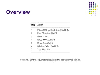
- 35. Microprogram Sequencing ’ü¼ If all microprograms require only straightforward sequential execution of microinstructions except for branches, letting a ╬╝PC governs the sequencing would be efficient. ’ü¼ However, two disadvantages: ’āś Having a separate microroutine for each machine instruction results in a large total number of microinstructions and a large control store. ’āś Longer execution time because it takes more time to carry out the required branches. ’ü¼ Example: Add src, Rdst ’ü¼ Four addressing modes: register, autoincrement, autodecrement, and indexed (with indirect forms).
- 36. - Bit-ORing - Wide-Branch Addressing - WMFC
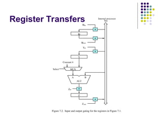
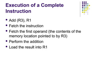
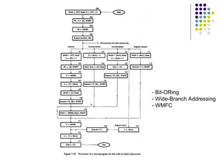
- 37. OP code 0 1 0 Rsrc Rdst Mode Contents of IR 0 3 4 7 8 10 11 Figure 7.21. Microinstruction for Add (Rsrc)+,Rdst. Note: Microinstruction at location 170 is not executed for this addressing mode. Address Microinstruction (octal) 000 PCout, MARin , Read, Select 4 , Add, Zin 001 Zout, PCin, Yin, WMFC 002 MDRout, IRin 003 ’üŁBranch { ’üŁ PC’é¼ 101 (from Instruction decoder); ’üŁPC5,4 ’é¼ [IR10,9]; ’üŁPC3 ’é¼ 121 Rsrcout, MARin , Read, Select4, Add, Z in 122 Zout , Rsrcin 123 170 MDRout, MARin , Read, WMFC 171 MDRout, Yin 172 Rdstout , SelectY , Add, Zin 173 Zout , Rdstin, End [IR10]’āŚ[IR9]’āŚ[IR8]} ’üŁBranch {’üŁPC’é¼ 170;’üŁPC0 ’é¼ [IR8]}, WMFC
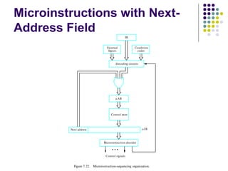
- 38. Microinstructions with Next- Address Field ’ü¼ The microprogram we discussed requires several branch microinstructions, which perform no useful operation in the datapath. ’ü¼ A powerful alternative approach is to include an address field as a part of every microinstruction to indicate the location of the next microinstruction to be fetched. ’ü¼ Pros: separate branch microinstructions are virtually eliminated; few limitations in assigning addresses to microinstructions. ’ü¼ Cons: additional bits for the address field (around 1/6)
- 39. Microinstructions with Next- Address Field Figure 7.22. Microinstruction-sequencing organization. Condition codes IR Decoding circuits Control store Next address Microinstruction decoder Control signals Inputs External ’üŁAR ’üŁIR
- 40. F1 (3 bits) 000: No transfer 001: PCout 010: MDRout 011: Zout 100: Rsrc out 101: Rdstout 110: TEMPout F0 F1 F2 F3 F0 (8 bits) F2 (3 bits) F3 (3 bits) 000: No transfer 001: PC in 010: IR in 011: Zin 100: Rsrc in 000: No transfer 001: MARin F4 F5 F6 F7 F5 (2 bits) F4 (4 bits) F6 (1 bit) 0000: Add 0001: Sub 0: SelectY 1: Select4 00: No action 01: Read Microinstruction Address of next microinstruction 101: Rdstin 010: MDRin 011: TEMP in 100: Yin 1111: XOR 10: Write F8 F9 F10 F8 (1 bit) F7 (1 bit) F9 (1 bit) F10 (1 bit) 0: No action 1: WMFC 0: No action 1: ORindsrc 0: No action 1: ORmode 0: NextAdrs 1: InstDec Figure 7.23. Format for microinstructions in the example of Section 7.5.3.
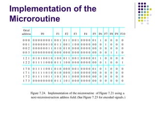
- 41. Implementation of the Microroutine (See Figure 7.23 for encoded signals.) Figure 7.24. Implementation of the microroutine of Figure 7.21 using a 1 0 1 1 1 1 1 0 0 1 1 1 1 1 0 0 0 1 0 0 1 1 2 1 0 0 0 0 0 0 0 0 0 0 0 0 0 0 0 0 0 0 0 0 0 0 0 0 0 1 0 1 1 1 0 3 7 7 0 0 0 0 0 0 0 0 0 1 1 1 1 1 1 0 0 0 0 1 7 0 7 F9 0 0 0 0 0 0 F10 0 0 0 0 0 0 0 0 0 0 0 0 0 0 F8 F7 F6 F5 F4 0 0 0 0 0 0 0 0 0 0 0 0 0 1 0 0 0 0 0 0 0 0 0 0 0 0 1 1 0 0 0 0 1 0 0 0 1 0 0 0 0 0 0 0 0 1 1 0 0 0 0 0 1 0 0 0 0 0 0 0 1 0 0 0 0 0 0 0 0 0 0 1 0 0 0 0 0 0 0 0 1 1 1 0 1 0 0 1 0 F2 1 1 1 0 0 0 0 0 0 1 1 2 2 1 0 1 1 1 1 0 1 1 1 0 0 1 1 2 0 2 1 0 0 0 address Octal 1 1 1 0 0 0 0 0 1 0 0 0 0 0 0 0 1 0 0 0 0 0 0 0 F0 F1 0 0 0 1 0 0 0 1 0 0 1 0 0 1 1 0 0 1 1 1 0 1 0 0 0 0 0 1 1 0 1 F3 next-microinstruction address field. 0 1 1 0 0 0 0 0 0 0 0 0 0 0 0 0 0 0 0 0 0 0 0 0 3 0 0 0 0 0 0
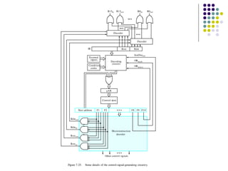
- 42. decoder Microinstruction Control store Next address F1 F2 Other control signals F10 F9 F8 Decoder Decoder circuits Decoding Condition External codes inputs Rsrc Rdst IR Rdstout Rdstin Rsrcout Rsrcin ’üŁAR InstDecout ORmode ORindsrc R15in R15out R0in R0out Figure 7.25. Some details of the control-signal-generating circuitry.
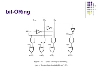
- 43. bit-ORing
- 44. Further Discussions ’ü¼ Prefetching ’ü¼ Emulation